Optimizing PCB Manufacturing with CCD Back-Drilled Leads
Printed circuit boards (PCBs) provide interconnections for electronic components and parts, forming modules or finished products with specific functions.
Printed circuit boards (PCBs) provide interconnections for electronic components and parts, forming modules or finished products with specific functions.
The principle of acid etching relies on the reaction between divalent copper in the etching solution and the metallic copper on the surface of the printed circuit board (PCB).
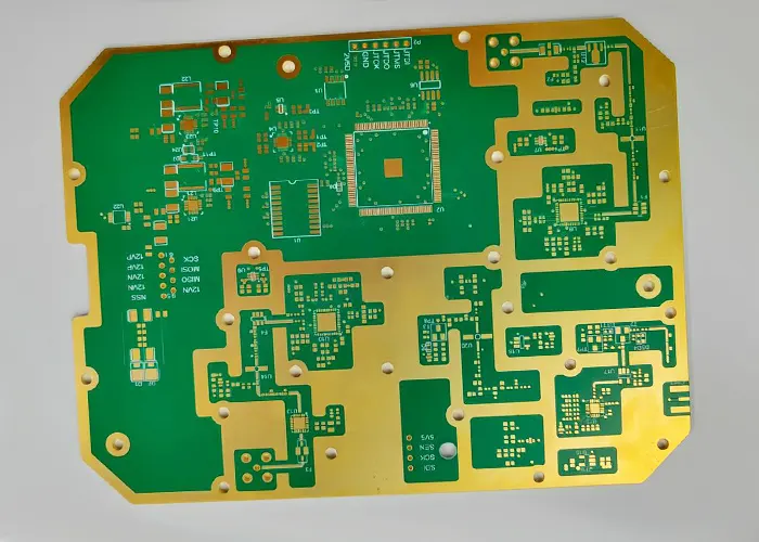
As the functionalization of multilayer printed circuit boards (PCBs) continues to advance, multilayer PCBs are often designed with stepped structures featuring varying board thicknesses.
In the era of rapid advancements in communication technology, terminal application scenarios are becoming increasingly diverse and undergoing continuous iteration and renewal.
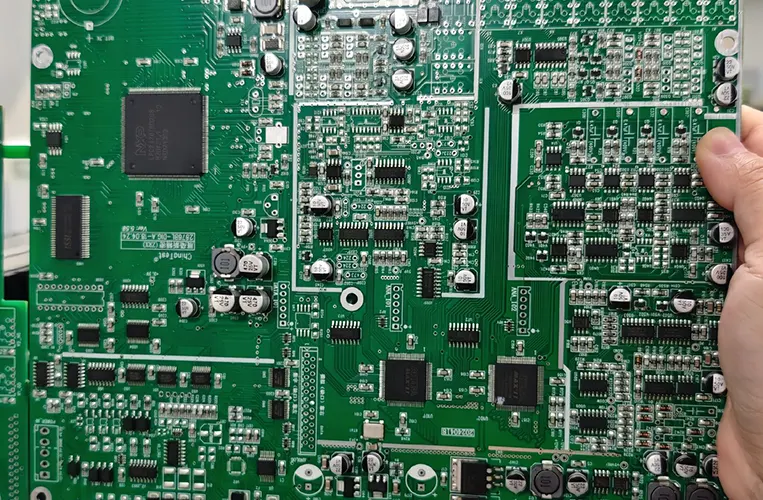
Printed circuit boards (PCBs) serve as fundamental components of electronic products, playing a crucial role in contemporary technology. With the advancement of 5G technology, communication systems demand ever-increasing speeds and capacities, thereby imposing stricter specifications on PCB substrate characteristics such as thickness, surface morphology, and impedance.
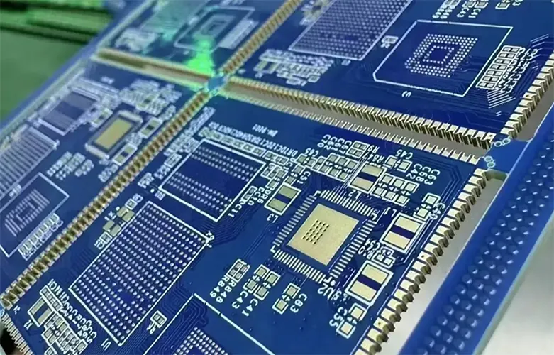
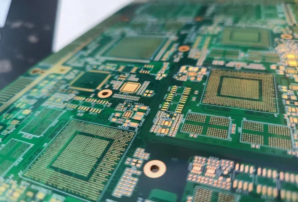
PCB stands for Printed Circuit Board, the abbreviated term for printed circuit boards. Typically, conductive patterns formed on insulating materials according to predetermined designs—either as printed circuits, printed components, or a combination of both—are referred to as printed circuits.
Printed circuit boards (PCBs), born in the 1940s, have seen the development of numerous distinct types over more than seventy years since their commercialization in the 1950s.
Reference points, also known as mark points or optical positioning points, are essential for precise PCB assembly in automated manufacturing. Serving as measurable coordinates for placement machines, these marks ensure accurate alignment of circuit patterns and components across all assembly stages.