
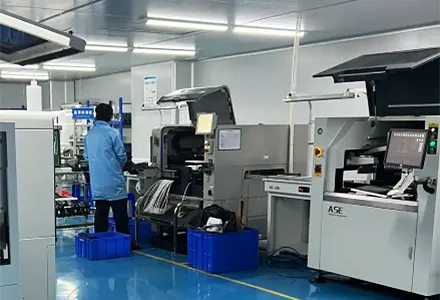
PCBA Assembly
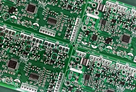
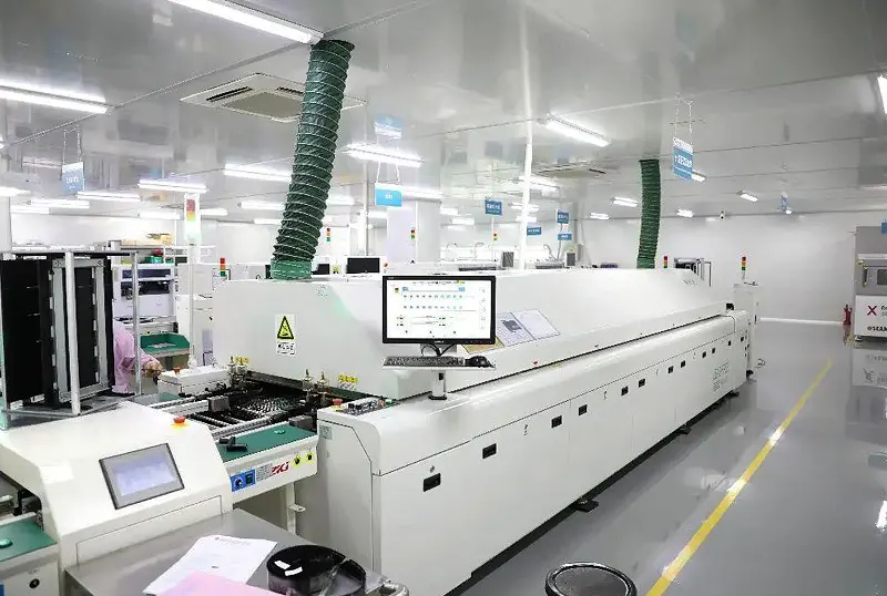
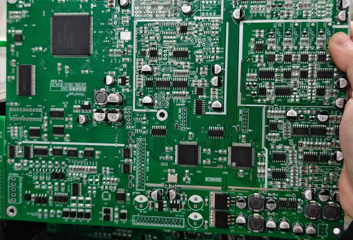
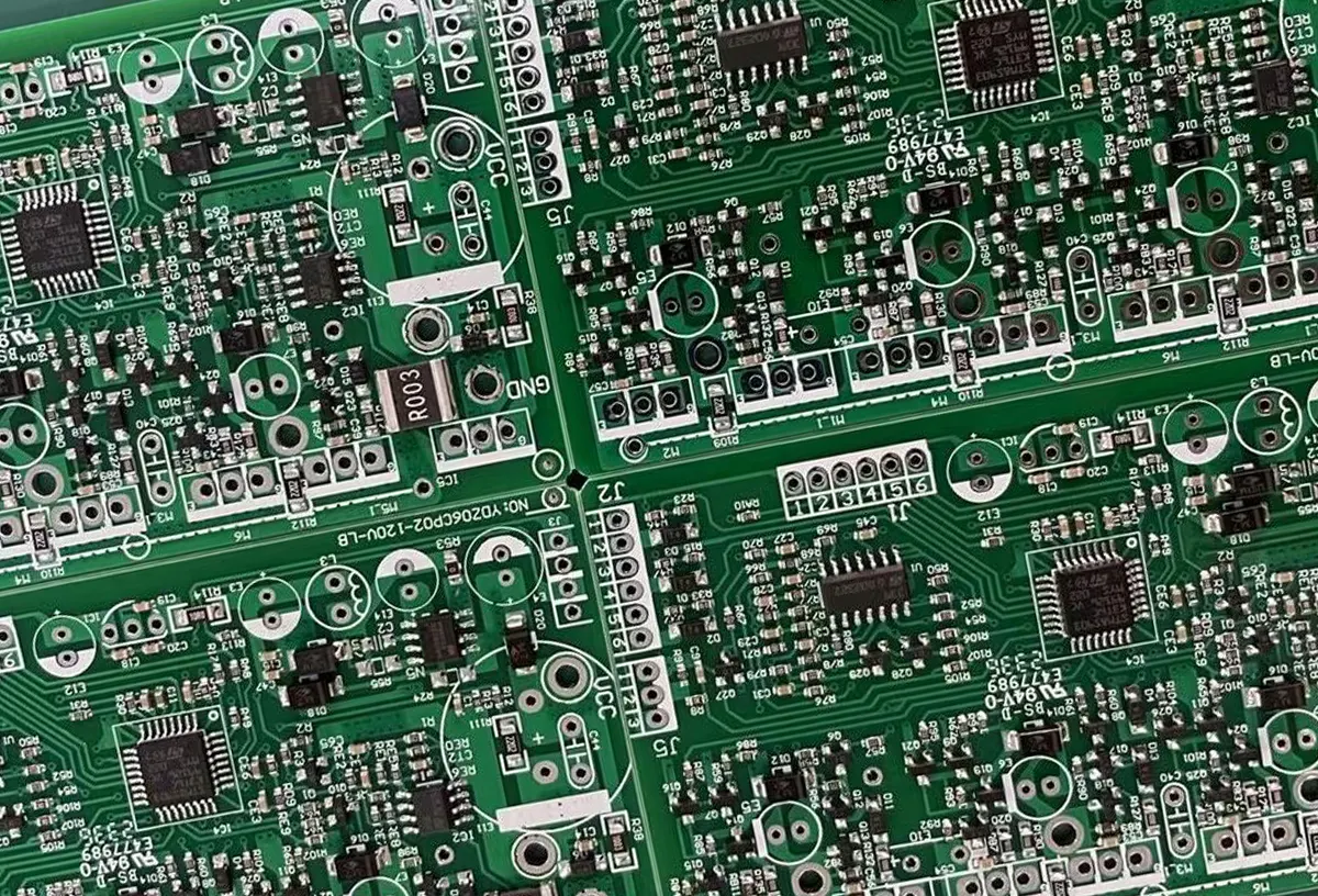
PCBA Assembly mounts electronic components onto PCBs, ensuring precision, reliability, and high performance across various industries. Ensure high quality to customer.
- Layers: 1-42 layers
- PCB Thickness: 0.3MM-4MM
- PCB Size: L*w:50*50–510mm*460mm
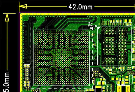
PCB Design
PCB Design is the process of creating circuit layouts that connect electronic components efficiently and reliably. It ensures optimal performance, manufacturability, and product quality for various electronic applications
- Typically Tooling: 30 days
- Typically injection molding: 3 days
- 1 to 1M pcs
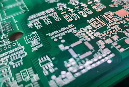
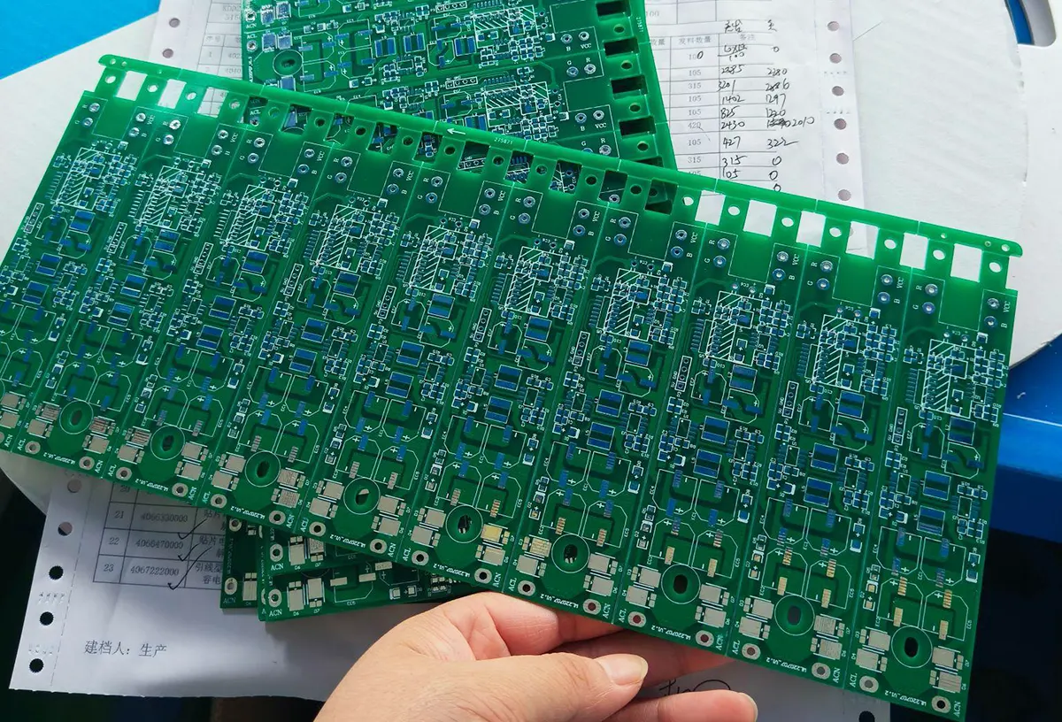
PCB Manufacturing
PCB Manufacturing is the process of producing printed circuit boards that connect and support electronic components. It ensures high precision, durability, and quality for reliable electronic products.
- Typical leading time 3 days.
- Typically +/- 0.15mm or +/-0.006 inch
- State-of-the-Art Technologies
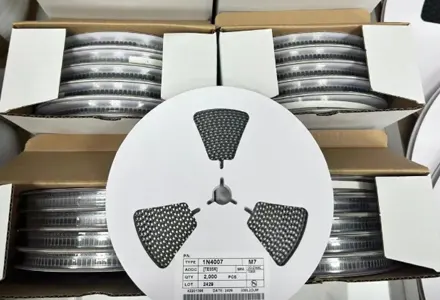
Procurment
Procurement is the process of sourcing and purchasing high-quality electronic components and materials needed for production. It ensures cost efficiency, reliability, and on-time delivery throughout the manufacturing process.
- Tolerances as tight as ±0.2 mm
- Machined parts lead time 1 day
- Max Size: 1400x700x500mm

Box Building
Box Building is the final stage of assembly, integrating PCBs, wiring, and enclosures into a complete, ready-to-use product. It ensures seamless functionality, durability, and professional finishing.
- Wall Thickness 0.8 mm
- Machined parts lead time 4~5 day
- Minimum Possible Batch 1000 pcs
Prototype Assembly
Prototype Assembly is the process of building and testing initial PCB samples to validate design and functionality before mass production. It ensures accuracy, reliability, and faster product development.
- Tolerances as tight as ±0.05 mm
- Wall Thickness 1.5mm~2.5mm
- Quantitites 25 copies per mold



PCB Layout Details: Corner Handling, Trace Width & Spacing for Mass Production
This article analyzes common pitfalls of PCB layout details including routing corners, trace width and trace spacing. It explains hidden issues undetectable by conventional DRC, together with real mass-production cases and standardized design workflows for hardware and layout engineers.

PCB Trace Width: Calculation Methods and Its Relationship with Current
This article introduces PCB trace width definition, calculation formulas and IPC standards. It explains the correlation between PCB trace width and current carrying capacity, impedance and signal reflection, together with practical layout cases for high-speed and power circuits.

PCB vs ABF Substrate: Core Differences, Manufacturing Process & Industry Chain
This article clarifies the distinctions between PCB and ABF substrate. Compare their scale, fabrication processes, materials, industrial positioning and common misconceptions, covering AI chip packaging and domestic substitution trends.