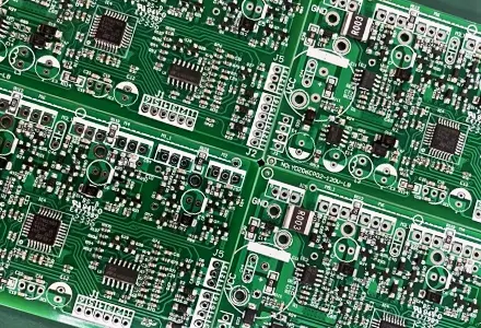
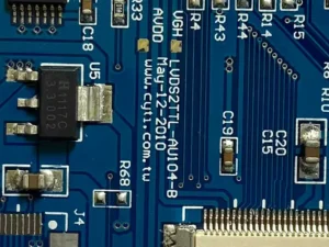
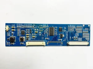
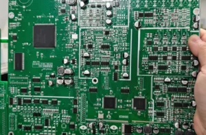
PCB fabrication is the process of transforming your electronic design into a real, functional circuit board—layer by layer, with precision and reliability. It blends engineering, materials science, and advanced manufacturing to create the backbone of every electronic product.
From smartphones and medical devices to industrial controllers and IoT systems, PCB fabrication brings ideas to life by turning schematics into high-performance, ready-to-assemble boards.
Why Choose Our PCB Fabrication Services?
Ready to build your next PCB? Contact us.
Reliable Quality Assurance
Strict inspections and certified processes ensure every PCB meets industry standards.
Advanced Manufacturing Capabilities
State-of-the-art equipment delivers precise, high-performance PCBs for any application.
Fast Turnaround Times
Efficient workflows and optimized production guarantee quick delivery without compromise.
Competitive Pricing
Cost-effective solutions that balance quality, performance, and budget.
ull Material Traceability
Every material is tracked to ensure transparency, reliability, and accountability.
Expert Engineering Support
Professional engineers provide guidance from design review to final production.
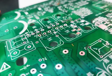
Our PCB Fabrication Capabilities
Ready to build your next PCB? Contact us.
PCB Types We Fabricate
Single-sided / Double-sided PCBs
Multilayer PCBs (up to 32 layers)
HDI PCBs
Rigid PCBs
Flex PCBs / Rigid-Flex PCBs
Aluminum / Copper boards
High-frequency PCBs
Manufacturing Capabilities
Minimum trace/space
Copper thickness options
Board thickness range
Hole sizes (PTH, NPTH)
Solder mask / surface finish options
Impedance control
HDI capabilities
Materials We Support
FR4
Rogers
Polyimide
Aluminum substrate
High-TG materials
Halogen-free materials
Others
PCB Fabrication Process
Ready to build your next PCB? Contact us.
Engineering review & DFM check
Item content. Click the edit button to change this text.
1
New Office, CA
Material preparation
Item content. Click the edit button to change this text.
2
New Office, CA
Inner layer imaging & etching
Item content. Click the edit button to change this text.
3
New Office, CA
Lamination
Item content. Click the edit button to change this text.
4
New Office, CA
Drilling
Item content. Click the edit button to change this text.
5
New Office, CA
Plating & copper deposition
Item content. Click the edit button to change this text.
6
New Office, CA
Outer layer imaging
Item content. Click the edit button to change this text.
7
New Office, CA
Etching
Item content. Click the edit button to change this text.
8
New Office, CA
Solder mask application
Item content. Click the edit button to change this text.
9
New Office, CA
Surface finish (ENIG, HASL, OSP…)
Item content. Click the edit button to change this text.
10
New Office, CA
Silkscreen printing
Item content. Click the edit button to change this text.
11
New Office, CA
Cutting & routing
Item content. Click the edit button to change this text.
12
New Office, CA
Final inspection & testing (E-test, AOI)
Item content. Click the edit button to change this text.