Failure analysis is a crucial component of product reliability engineering. It is widely applied to determine the causes of production issues during development and manufacturing, identify reliability-related failures during testing, and confirm the mechanisms of field failures during use.
By drawing lessons from case studies, it proposes recommendations for improving design and manufacturing processes, preventing recurrence of failures, and enhancing product reliability.
Solderability and Failure Modes
Solderability
The ability of metallic materials such as copper, nickel, gold, silver, and tin to form high-quality joints through welding under specific process conditions is termed solderability.
During welding, the solder and base metals undergo atomic bonding, penetration, migration, and diffusion under high temperatures, forming an intermetallic compound (IMC).
The formation and subsequent quality of this IMC directly impact the reliability of the welded joint.
Solderability Failure Modes
The primary solderability failure modes in printed circuit board assembly (PCBA) include: poor wetting, tombstoning, cracking, porosity, cold solder joints, incomplete solder wetting, and slag inclusion defects.
Key Factors Contributing to PCBA Soldering Failures
Quality of Raw Materials: Flux, Solder, etc.
Soldering materials primarily consist of flux and solder. The flux must effectively remove oxide layers from the surfaces of the metals and solder being joined.
Solder connects two or more metal surfaces and simultaneously forms a metallurgical bond between them.
Engineers must select the appropriate solder based on the specific components being joined and the prevailing soldering conditions.
Influence of Welding Process Conditions
Operators must appropriately control time and temperature to ensure uniform heating.
Generally, higher temperatures enhance wetting properties, while the duration affects the formation of intermetallic compound structures.
PCB Quality
The surface of printed circuit boards (PCBs) must remain clean.
The presence of oxidation layers, dust, or oil contamination on the PCB surface will adversely affect the formation of the alloy layer around soldered components.
Failure Analysis Method
Information Gathering
Failure analysis begins with the failure phenomenon, involving the collection of background information and selection of samples for analysis.
Through information gathering, functional testing, electrical performance testing, and simple visual inspection, engineers identify the failure location and mode to determine failure localization and fault location.
Analytical Techniques
For more complex failure phenomena, the location of defects that are difficult to observe requires the use of other auxiliary tools for determination.
These include visual inspection using microscopes, X-ray radiography, metallographic section analysis, thermal analysis, micro-infrared analysis, scanning electron microscopy (SEM), and X-ray energy dispersive spectroscopy (EDS).
Among these, metallographic section analysis is a destructive analytical technique; scanning electron microscopy and X-ray energy dispersive spectroscopy may also require partial destruction of the sample.
During the analysis process, engineers may employ additional testing techniques to locate failures and validate their causes.
These include thermal stress testing, electrical property testing, solderability testing, and dimensional measurement.
Experimental Verification
Engineers can identify the precise cause of failure through experimental verification methods and comparative analysis.
If conditions permit, engineers may also conduct simulation tests to reproduce the failure process and validate the reliability of the failure analysis results.
This provides a basis for subsequent improvements.
Data Analysis
Compile a failure analysis report based on evidence and conclusions derived from experimental data, comparative analysis, and validation information obtained during the analysis process.
Throughout the analysis, ensure data authenticity and logical coherence.
Adhere to the principle of employing analytical methods progressively—from simple to complex, from external to internal, and from non-destructive to destructive techniques.
This systematic approach is the only way to avoid erroneous judgments and incorrect failure mechanisms.
Solderability Failure Analysis Case Study
Background
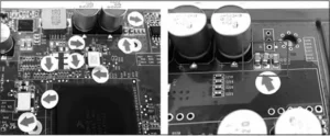
After surface mount technology (SMT) component placement and soldering, lead-free hot air solder leveling (HASL) PCBs exhibited poor wettability at pad locations, with a defect rate of 56.25%, as shown in Figure 1.
Failure Analysis Steps for Poor Weldability Defect Boards
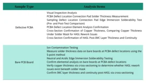
Based on the collected failure conditions of PCBA (Printed Circuit Board Assembly), establish analysis items (as shown in Table 1).
Analysis and Verification
The following sections describe visual inspection and process verification.
1. Visual Analysis
Visual inspection of the failed samples indicates that solderability issues primarily occurred on the C-side (BGA side), with no defects observed on the S-side.
Additionally, engineers confirmed that the client’s SMT (Surface Mount Technology) process first solders the S-side during the initial reflow.
The defective C-side (BGA side) undergoes a second reflow.
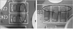
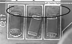
Poor solderability manifested as insufficient wettability of the connection pads during the second reflow, resulting in components deviating from their pads, as shown in Figure 2.
2. Solder Thickness Measurement Confirmation at Defective Locations on PCBA
Table 2 and Figure 3 show the solder thickness measurements at wettability failure locations for defective PCBA samples.
The results meet requirements, with solder thickness data falling near the lower limit value.

3. Perform Edge Solderability Testing on Poorly Sampled Locations Using the Edge Solder Immersion Method
Resample non-wetting areas on defective PCBA boards and conduct edge solder immersion tests using neutral flux (Type A flux). Observation indicates satisfactory solderability.
4. Elemental Analysis Confirmation of PCBA Defective Locations
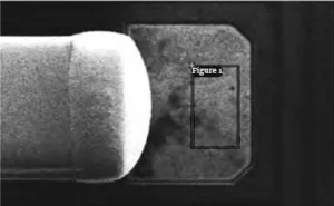
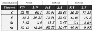
For pads with poor wetting (as shown in Figure 4), engineers performed EDS (Energy Dispersive X-ray Spectrometer) elemental analysis at three locations.
Copper content was normal (as shown in Figure 5), with no abnormal elements detected.
5. HASL Rework Verification for PCB
Due to copper dissolution issues during HASL processing, typical normal HASL results in 1–3 μm copper dissolution.
Cross-section analysis confirmed the difference in copper thickness under solder pads versus HASL areas.
Soldering process caused approximately 2 μm copper dissolution. Cross-section analysis revealed copper thickness of 51.45 μm under solder mask and 47.80 μm in HASL areas.
The difference between the two copper thicknesses is 3.65μm. Therefore, it can be determined that no rework issues occurred during the process.
6. Cross-Section Analysis Confirms IMC Layer Thickness and Continuity After Hot-Air Solder Leveling
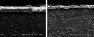
SEM observation reveals a continuous IMC layer at the defective pad location.
However, due to the solder thickness being at the lower limit (1.5–2.1 μm), the entire solder layer has undergone IMC conversion.
Cross-section analysis (as shown in Figure 6) further revealed that the thinner solder areas had entirely formed an IMC layer with extremely poor wettability.
At the 8mm position on the PCB, a good solder surface remained above the IMC layer with excellent wettability.
The primary cause was that the thin solder layer prevented proper alloying and wetting during hot-air solder leveling, leading to solder shrinkage.
7. Verification Analysis of Bare PCB Boards in Stock
Engineers conducted ion contamination testing on PCB boards from inventory and obtained satisfactory results (as shown in Table 3).
This further confirms that the bare PCB boards have not suffered external contamination that could cause poor solderability.

8. Solder Thickness Measurement at Corresponding Bare PCB Locations for PCBA Defective Areas
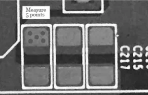
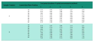
Engineers measured the solder thickness on the bare board using the five-point method (as shown in Figure 7) by comparing the upper limit defective areas on the PCBA.
Test results generally meet specification requirements, as shown in Table 4. The specification requires 1–40 μm, with only a few solder thicknesses falling near the lower limit.
9. Solderability Testing Using Neutral and Acidic Edge-Dipping Methods
Two stock PCBs underwent two lead-free reflow soldering cycles, simulating customer SMT placement on both sides.
Engineers then tested the samples for solderability and obtained the following results:
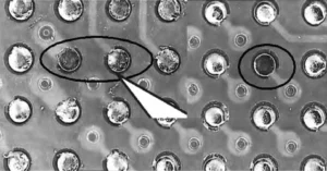
- Neutral flux (Type A): Microscopic examination revealed numerous solder voids on the BGA connection pads, as shown in Figure 8;
- Acidic flux: Microscopic examination revealed isolated instances of poor solder wetting.
10. Elemental Analysis Verification
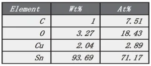
Engineers performed EDS elemental analysis on the bare PCB board at the PCBA defect location.
They detected no abnormal elements (as shown in Figure 9), and the copper content was normal.
Summary of Analysis Results
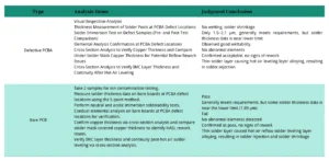
The summary of analysis results is shown in Table 5.
Analysis Conclusions
(1) Based on the comparative data above:
– PCBA: The IMC layer at solder-rejected pads appears continuous, but the solder thickness is at the lower limit (1.5–2.1 μm), resulting in complete IMC formation across the entire solder layer. PCB: On bare boards, the IMC layer formed across the entire range of 1–2 μm solder thickness, exhibiting extremely poor wettability.
For bare boards with solder thickness above 2 μm, a good solder surface remained above the IMC layer, demonstrating relatively better wettability.
The primary cause of solder rejection on PCBA after soldering is the failure of HASL layers to wet due to inconsistent solder thickness.
(2) Lead-free HASL boards primarily using SAC305: During the client’s first-side reflow soldering, wettability with the solder paste was reasonably good.
However, severe solder rejection and lack of wettability occurred during the second-side reflow soldering.
(3) HASL boards develop a Cu6Sn5 intermetallic compound (IMC) layer during processing.
By the time the PCB undergoes the second reflow at the client site, this marks the third instance of IMC growth.
Since the HASL layer exposed to solder paste during the client’s second reflow contains no pure tin (due to the solder thickness being near the lower limit), soldering relies entirely on the 50% solderability of the IMC, leading to poor wetting.
(4) Strictly control HASL thickness at the midpoint and reduce solder bath temperature (as higher temperatures accelerate IMC growth and increase its porosity).

