When designing multilayer circuits requiring impedance control, printed circuit board (PCB) designers must collaborate closely with engineers experienced in radio frequency (RF) PCB layout, including mixed-signal application specialists.
RF engineers can provide PCB designers with “best practice” guidance when planning RF circuit boards and corresponding manufacturing guidelines for specific components.
They can recommend qualified PCB manufacturers and specify substrate and copper foil materials suitable for the application.
Controlled impedance is the characteristic impedance of a transmission conductor relative to a reference plane.
Impedance control is most critical when high-frequency signals traverse transmission lines across adjacent layers of an RF circuit; consistent controlled impedance is essential for achieving signal integrity and delivering signals with minimal distortion.
RF engineers can guide PCB designers in determining the thickness and placement of copper-clad glass-fiber reinforced core materials within the layup scheme, as well as specifying the thickness of prepreg materials used for interconnect layers during lamination.
A critical issue is determining the thickness of the dielectric core material.
Dielectric thickness dictates the physical distance between conductors on signal layers and the “reference plane” layer.
Below are some “best practices” provided by RF engineering design experts.
RF Transmission Conductors
Care must be taken to prevent unintended coupling between signal conductors. Spacing between conductors should be maximized, avoiding long runs in close proximity.
Coupling between parallel microstrip conductors increases as spacing decreases and the length of parallel routing increases.
Conductors crossing between different circuit layers should have a copper ground plane to provide isolation.
Conductors carrying high power levels should be isolated from all other signal conductors as much as possible.
High-Speed Digital Signal Conductors
High-speed digital signal traces should be routed on a separate layer from RF signal traces to prevent coupling.
Digital noise (originating from the phase-locked loop, PLL) can couple onto RF signal traces and modulate the RF carrier. Additionally, in certain circumstances, digital noise may undergo up/down conversion.
Power Supply and Ground Decoupling
Install decoupling/bypass capacitors at the main power supply voltage distribution nodes and at power supply voltage branches.
Select the bypass capacitor values based on the overall frequency response of the RF integrated circuit and the expected frequency distribution characteristics of any digital noise from the clock and PL.
These power lines should also be separated from any RF lines that will carry significant RF power.
Conductor Planning for RF Applications
There are two fundamental types of conductors for transmitting RF signals: microstrip and stripline.
The primary distinction between these two conductor types lies in the position of the signal conductor relative to the reference plane.
Impedance control becomes paramount when high-frequency signals cross adjacent transmission lines.
Microstrip conductors are routed on the outer surface of the substrate, while stripline conductors are sandwiched between two reference planes.
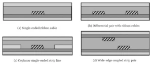
A typical transmission line for controlled impedance applications using stripline is shown in Figure 1.
Stripline functions identically to microstrip, but the RF signal is enclosed by ground planes on both the top and bottom.
These ground planes provide isolation to minimize external interference to the microstrip via RF signal transmission.

The spacing between two conductors in a differential pair should not exceed twice the conductor width.
For example, the distance between differential conductors 0.10mm wide should not exceed 0.20mm.
The width of a single conductor should not exceed twice the dielectric thickness between adjacent signal layers and ground planes.
High-Frequency RF Signal Issues
For VHF circuit applications, the smoothness of conductor surfaces is a primary concern.
To address this issue, copper foil suppliers strive to provide superior surfaces.
To maximize adhesion between copper and dielectric materials, an oxide replacement bonding treatment has been introduced.
When applied to inner layer conductors prior to lamination, it delivers a smoother surface.
Signal Line Isolation
Care must be taken to prevent unintended coupling between signal lines.
Measures to prevent potential coupling include: RF transmission conductors should be spaced as far apart as possible, avoiding long runs in close proximity.
Coupling between parallel microstrip lines increases as spacing decreases and the distance between parallel traces increases.
Conductors crossing on different layers should be separated by a ground plane.
Signal conductors carrying high power should be routed as far away as possible from all other traces.
Ground coplanar waveguides provide excellent isolation between lines. Achieving better than approximately -45 dB isolation between RF conductors on small PCBs is impractical.
Ground Plane
Assuming Layer 1 is used for RF components and transmission lines, a solid (continuous) ground plane is recommended on Layer 2.
For striplines and skewed stripline variants, ground planes are required above and below the center conductor.
These planes must not be shared or allocated to signal or power networks; they must be dedicated solely to ground.
Partial ground planes on a layer, sometimes required by design constraints, must be located beneath all RF components and transmission lines.
The ground plane beneath transmission line routing must be continuous.
Additionally, numerous interlayer ground vias should be added throughout the RF section of the PCB to help prevent parasitic ground inductance caused by ground current return paths.
These vias also help prevent cross-coupling between RF and other signal traces on the PCB.
Special Considerations for Bias and Ground Planes
Layers allocated for system bias (DC power supply) and ground must be determined based on the component’s return current.
A general guideline is to avoid routing signals on layers between the bias plane and the ground plane.
Power Supply (Biased) Routing and Power Decoupling
When a single component has multiple power connections, a common approach is to implement a “star” configuration for power routing.
Larger decoupling capacitors (tens of μF) are placed at the “root” of the star, while smaller capacitors are installed on each branch.
The value of the smaller capacitors depends on the RFIC’s operating frequency range and its specific functionality (i.e., decoupling between stages and the main power supply).
Selecting Decoupling or Bypass Capacitors
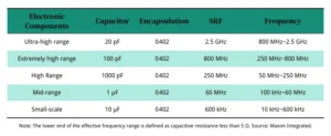
Due to the self-resonant frequency (SRF) inherent in actual capacitors, their effective frequency range is limited: SRF values can be obtained from manufacturers, but sometimes require direct measurement for characterization.
At the SRF, the capacitor exhibits inductive behavior and thus fails to perform decoupling or bypassing functions.
For broadband decoupling, the standard approach involves using multiple capacitors of progressively larger values, connected in parallel.
Smaller capacitors typically have higher SRFs (e.g., 0.2 pF in a 0402 SMT package with an SRF of 14 GHz), while larger capacitors have lower SRFs (e.g., 2 pF in the same package with an SRF of 4 GHz).
Refer to Table 1 for capacitance value selection guidelines.

Note: The lower end of the effective frequency range is defined as capacitive reactance less than 52. Source: Maxim Integrated
Layout Considerations for Bypass Capacitors
Power lines must be AC-grounded, making it critical to minimize parasitic inductance introduced into the AC ground loop.
Such inductance may arise from layout choices or component orientation, such as the grounding orientation of decoupling capacitors.
Connecting the top-layer power voltage pad to an internal power plane (layer) via a through-hole may impede the return path for AC ground currents, forcing a longer return route and resulting in higher parasitic inductance.
Any AC current flowing into the power voltage pin will reach its ground side via the bypass capacitor before returning to the internal ground plane.
This configuration provides the smallest total footprint for the bypass capacitor and associated through-hole.
Conclusion
Designers collaborating with companies developing RF-dominant products may have accumulated extensive experience in radio frequency, but for most, further learning is still required.
To prepare for developing circuit boards that require impedance control, designers can obtain extensive guidance from their designated PCB suppliers—the companies responsible for manufacturing the actual boards.


