With the rapid advancement of electronic power technology, DC/DC power modules have developed significantly.
They are now widely adopted in high-end equipment across aerospace, power electronics, 5G communications, and military electronics.
These systems impose extremely stringent requirements on the size and weight of core components like DC power modules.
Moreover, the module power supply must feature highly reliable thermal management to meet high conversion efficiency specifications, ensuring long-term stable operation of both the power module and the entire system.
Consequently, power modules will inevitably evolve toward miniaturization, lightweight design, high power density, and high efficiency.
Achieving the high power density and high efficiency technical specifications of module power supplies necessitates support from advanced packaging processes.
Currently, some power modules typically employ open-board or potting-type packaging structures.In these designs, components are distributed on a PCB.
Potting-type enclosures use plastic and metal materials, and the interior cavity is fully filled with high-thermal-conductivity silicone rubber.
Such packaging structures suffer from drawbacks including large volume, heavy weight, and poor heat dissipation, failing to meet the technical demands of high-end electronic equipment for high-power-density power modules.
In contrast, some countries have adopted advanced monolithic plastic encapsulation technology.
This technology not only reduces the volume and weight of power modules but also enhances thermal efficiency.
It increases power density by several times and demonstrates significant technological advantages.
A newly developed half-brick 1000W high-power power module features high assembly density, large planar dimensions, and substantial overall thickness.
Traditional open-board or potting encapsulation structures cannot simultaneously meet the product’s dimensional requirements and high-reliability thermal management demands.
Therefore, this study innovatively employs an integrated plastic encapsulation process for double-sided injection molding of the power supply module.
The resulting high-power-density plastic-encapsulated power supply module with superior performance provides significant guidance for research on plastic encapsulation techniques for board-level power supply modules.
Preparation of Power Module PCBA for Encapsulation
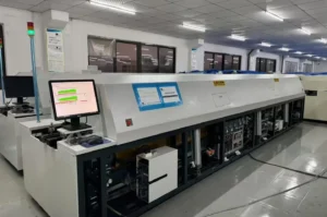
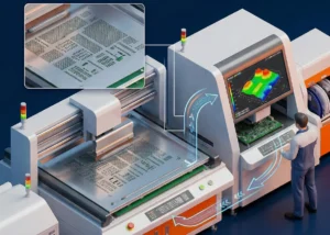
The power module PCBA for encapsulation is a high-power-density product.Figure 1 shows its assembly process flow.
Technicians assemble surface-mount components onto both the upper and lower surfaces of the PCB using reflow soldering.
They install board-level magnetic cores into corresponding openings on the PCB through an adhesive bonding process.

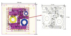
Figure 2 shows the schematic diagram of the PCBA product’s planar structure.
The PCB frame adopts a single-board design with a thickness of 2.8mm and external dimensions of 100mm x 88mm.
The module’s components are densely assembled within a rectangular area measuring 61mm x 63mm.
With a power rating of up to 1000W, this power supply module imposes stringent thermal dissipation requirements on its packaging structure.
Optimal Selection of Epoxy Molding Compounds
Epoxy Molding Compound (EMC) is a single-component thermosetting resin material characterized by superior mechanical properties, excellent chemical resistance, and high electrical insulation strength.
It serves as the primary encapsulation material in electronic molding processes.
The selection of EMC for power modules forms the foundation of module molding technology, directly determining the encapsulation quality of power supply modules.
The selection of EMC material is closely related to the structural dimensions, mold design, and electrical characteristics of the molded product.
Unlike single-sided encapsulation for chips, power modules employ a double-sided encapsulation process.
Given their large structural dimensions and high thickness, the epoxy molding compound must exhibit good flowability.
Modules feature high power density, operate at elevated temperatures, and demand stringent heat dissipation, necessitating that the molding compound possess high thermal conductivity and excellent heat resistance.
Furthermore, the overall encapsulation of large-sized products requires low internal stress after EMC curing.
This ensures the encapsulation interface does not generate significant thermal stress or strain under high-temperature or thermal cycling conditions, thereby preventing accelerated delamination deterioration.
Consequently, the EMC for power supply modules must simultaneously meet parameters including high flowability, high thermal conductivity, high glass transition temperature (Tg), low coefficient of thermal expansion (CTE), and low modulus.
Table 1 presents the performance parameters of three preferred novel high-thermal-conductivity encapsulants.
Based on the comprehensive encapsulation requirements for this power module, Material Type B is selected for its balanced advantages: good flowability, high thermal conductivity, high Tg, and low stress.

Plastic Encapsulation Process Flow for Power Modules
-
Plastic Encapsulation Model for Power Modules
The primary challenges in plastic encapsulation for large-sized, high-thickness board-level power modules lie in mold design, process flow, and parameter optimization for double-sided integral encapsulation.
Based on the 3D structure of the PCBA product, the design team will employ a mold with dual injection ports and a single runner to encapsulate both sides of the power module simultaneously.
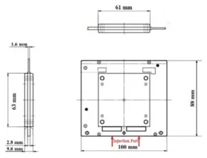
Figure 3 shows the encapsulation structure model of the module PCB frame.
The planar dimensions of the encapsulation area are 61 mm × 63 mm, with an overall thickness of 9.8 mm for double-sided encapsulation and a single-sided encapsulation height of 3.5 mm.
During power module injection molding, the encapsulation material simultaneously reaches the upper and lower surfaces of the PCBA through the gates, filling both cavities.
Once the mold fills, the process simultaneously encapsulates both sides of the module.
This design prevents pressure differentials caused by asynchronous injection on the upper and lower surfaces, thereby avoiding deformation or warping of the module’s PCB substrate due to unilateral pressure.
This prevents cracking or failure of device leads or solder joints.
-
Plastic Encapsulation Process Flow Design
Figure 4 illustrates the plastic encapsulation process flow for power modules.
Prior to encapsulation, PCBA products undergo a pre-baking treatment at 110°C for 4 hours to remove moisture from the substrate, reducing the risk of delamination at the encapsulation interface or substrate deformation.
The plasma cleaning process removes oxides and contaminants from the surfaces of the frame and components, enhancing the bonding strength at the encapsulation interface.
Following encapsulation, modules undergo a post-curing treatment at 175°C for 4 hours.
This facilitates complete curing of the encapsulant, further enhancing the physical, mechanical, and thermal properties of the encapsulated product while releasing residual stresses within the encapsulated body.

Optimization of Power Module Plastic Encapsulation Process Parameters
The team conducted a collaborative analysis to ensure that the plastic encapsulation process aligns with the selected epoxy encapsulant, PCBA frame, and mold structure.
This analysis involved both mold manufacturers and material suppliers.
This involved mold flow simulation and stress simulation of the encapsulation process.
These simulations yielded the optimal encapsulation parameters:
- * Mold temperature: 170–175 °C
- * Injection pressure: 800–1,000 N/cm²
- * Clamping force: 800–1,000 kN
- * Injection time: 20–25 seconds
- * Curing time: 180–200 seconds
Conducting potting tests within this injection parameter window effectively reduces trial-mold costs for power module potting.
It also enhances product validation reliability.
However, during actual trial production, defects such as overflow, frame deformation/fracture, and incomplete filling occurred in the potted power modules.
This paper proposes corresponding optimization directions for the potting process parameters.
After multiple rounds of parameter refinement, the potted encapsulation bodies achieved qualified appearance and good quality.
-
Overflow Defect in Molded Power Modules
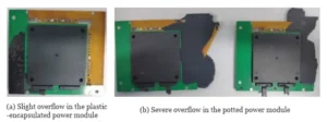
Figure 5 shows a defective molded power supply module with overflow. Overflow during the molding process is difficult to completely prevent, and minor overflow is normal and does not affect product performance.
However, severe overflow can damage equipment molds, compromise product appearance, and impact subsequent processes.
Possible causes of overflow defects include several factors.
One cause is the slow reaction speed of the molding compound, which results in a prolonged gelation time.
Another cause is excessive injection pressure, which leads to rapid material flow.
Insufficient clamping force can also contribute to overflow.
Large gaps between the mold and the PCB may cause the same issue.
These factors allow liquid encapsulant to overflow from the mold parting line.
To mitigate overflow defects in power modules, optimize encapsulation parameters as outlined in Table 2: Increase mold temperature to accelerate material curing and reduce flowability;
Extend preheating time for the encapsulant column to enhance reaction speed; Reduce injection pressure while increasing clamping pressure; decrease injection speed to increase flow resistance and slow material velocity.
Additionally, verify PCB board thickness consistency prior to encapsulation.
If board thickness falls below the design range (h=2.8±0.05 mm), replace thinner boards or compensate using epoxy shims of corresponding thickness.

-
Deformed and Fractured Board Frame in Molded Power Module
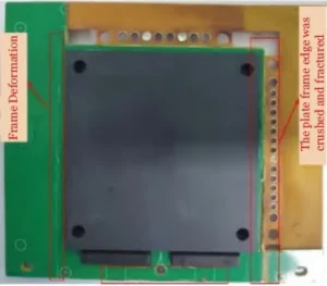
Figure 6 shows a defective molded power supply module with deformed and fractured board frame.
After molding, the PCB board frame exhibited significant deformation and fracture.
The process crushed and damaged local areas of the solder mask, and it fractured the board frame near the input/output through-hole pads.
This disrupted internal circuit connections, rendering the product inoperable and scrapped.
This defect likely resulted from excessive clamping pressure and injection pressure during molding, causing compressive and shear forces exceeding the PCB’s strength.
It may also relate to PCB thickness exceeding design specifications.
Excessively thick PCBs subjected to clamping forces exceeding design limits during molding caused deformation or fracture under improper external forces.
To resolve PCB frame deformation or fracture in molded power modules, it is necessary to optimize the injection molding parameters as outlined in Table 2.
One recommended measure is to reduce the clamping pressure to decrease the compression applied by the mold surfaces on the upper and lower sides of the PCB.
Lower injection pressure to minimize shear force from molten plastic during injection;
When the pressure and shear forces acting on the board frame are below its material strength, the board frame will not develop defects such as indentations, deformation, or fracture.
Additionally, prior to injection molding, the PCB board thickness must be verified to ensure it falls within the design tolerance (h=2.8±0.05mm). Products exceeding this thickness range must be rejected.
-
Unfilled Defects in Molded Power Modules
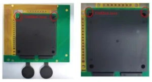
Figure 7 illustrates unfilled defects in a molded power supply module.
The unfilled areas concentrate near the filling tail on the underside of the PCBA and distribute around the screw holes.
This represents a common pattern of incomplete filling.
Such defects in molded modules primarily result from insufficient flow of the liquid encapsulant. At elevated temperatures, the reaction rate of the encapsulant accelerates, reducing gelation time.
The viscosity of the liquid encapsulant rapidly increases, leading to higher flow resistance. This causes the encapsulant to solidify before fully filling the mold cavity.
Additionally, excessive clamping pressure can also result in poor filling.
After entering the cavity, the liquid encapsulant encounters significant gas pressure resistance in confined spaces, preventing gas escape and preventing complete cavity filling.
This power supply module product features large planar dimensions, high thickness, and substantial potting compound usage, resulting in a long injection stroke.
During injection, flow resistance increases with distance traveled, peaking at the filling tail end beneath the PCB assembly (PCBA).
This location is particularly prone to filling defects.
If the injection time is too short, the potting compound rapidly fills the venting areas of the mold cavity.
This rapid filling impairs internal gas venting and flow, which also leads to filling defects.
Conversely, if the injection time is too long, the potting compound solidifies before reaching the trailing edge, resulting in missing potting material at the end.
Consequently, the design team sets the injection molding process parameter window for this product with strict tolerances.
To address the product’s tendency for unfilled defects, engineers can adjust and optimize the potting process parameters in several ways, as outlined in Table 2.
Reducing mold temperature increases the gelation time of the potting compound, slowing the reaction rate and improving the flowability of the liquid potting material.
Meanwhile, increasing injection pressure and injection speed while reducing clamping pressure promotes smoother flow of the liquid potting material within the gate and cavity.
This reduces resistance, facilitates efficient gas venting, ensures complete cavity filling, and results in a denser potting compound structure.
-
Well-molded Plastic-encapsulated Module Products
To address defects occurring during plastic encapsulation, the team analyzed the underlying mechanisms and implemented corresponding process improvement measures.
The plastic encapsulation process parameter window was standardized as follows: mold temperature 170–173°C, injection pressure 1,000 N/cm², clamping force 900 kN, injection time 22 seconds, and curing time 180 seconds.
Through continuous optimization of process parameters, this study successfully produced plastic-encapsulated power supply modules.
These modules exhibit excellent appearance, high quality consistency, and reliable electrical performance.
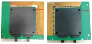
Figure 8 shows the appearance of a well-encapsulated power supply module. The encapsulated body exhibits no defects, with a smooth, crack-free surface and no contamination.
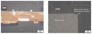
The team conducted a cross-sectional analysis of this encapsulated module to examine the microstructure at the encapsulation interface and within the encapsulant.
Figure 9 displays the microstructure of the product’s cross-section.
It reveals a dense internal molding structure with tight bonding at the interfaces between the molding compound and the PCB substrate, components, and magnetic core.
No defects such as delamination, voids, or cracks were observed.
Conclusion
This paper employs transfer molding with epoxy potting compound to achieve integrated injection molding of large-sized, high-thickness power supply modules.
The team selected an epoxy potting compound to meet the packaging requirements for efficient heat dissipation, simultaneous double-sided potting, and low thermal stress.
This compound offers high thermal conductivity, a high glass transition temperature, high fluidity, and low stress.
Addressing defects such as overflow, mold frame deformation or fracture, and incomplete filling observed during power module encapsulation trials, this paper conducts an in-depth analysis.
It examines the mechanisms behind these three types of defects.It also proposes corresponding process optimization measures.
Through continuous refinement of the encapsulation process flow and parameters, encapsulated power modules with sound encapsulation quality and normal electrical performance were successfully produced.
This work lays a crucial foundation for research into encapsulation process technology for large-sized, high-thickness power modules.

