Reference points, also known as mark points or optical positioning points, are essential for precise PCB assembly in automated manufacturing.
Serving as measurable coordinates for placement machines, these marks ensure accurate alignment of circuit patterns and components across all assembly stages.
By providing a reliable reference for automated systems, mark points minimize human error, improve placement precision, and enhance overall production efficiency.
Proper design, placement, and recognition of these marks are critical for achieving high-quality, high-volume PCB manufacturing.
Reference Point (Mark Point)
A mark point, also known as a reference point or optical positioning point, serves as the positioning reference for placement machines during operation.
In high-volume PCB production, it provides a common measurable point for all assembly steps.
This enables every device used in assembly to accurately position the circuit pattern for precision. Through the mark point, programmers can automatically configure the machine after loading the program.

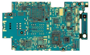
The Role of Mark Points on PCB Boards
When we send boards for manufacturing, we provide the Gerber files to the manufacturer.
If you need to assemble components onto the PCB, we also supply a Bill of Materials (BOM file) and a coordinate file (PNP file).
These files are used by automated placement machines to retrieve the necessary information, which then requires locating one or more actual physical points on the PCB.
Using mark points on the circuit board enables the machine to place components more accurately, achieving higher precision without relying on machine tolerances or human error.

Mark Point Recognition Principle
Mark points on PCBs serve as reference standards for automated machinery such as Surface Mount Technology (SMT) and Automated Optical Inspection (AOI).
This mark consists of an isolated copper pad distant from any other visible landmarks.
Without a reference mark, the machine will either place components incorrectly or refuse to operate altogether.
However, by reading the positions of various reference marks placed on the PCB, automated equipment can determine the precise location for placing or scanning components.
Technically, most machines do not read the content printed on the PCB. Instead, they detect the reflection from the mark pad.

Different Types of Mark Points
1. Single-Board Mark Points
Global mark points serve to locate all circuit features on a single board, distinguishing circuit graphics from the PCB reference plane.
We position them using three network systems, setting the reference point at the lower-left corner (0.0) and placing the other two along the positive directions of the X and Y axes.

2. Local Mark Points
Primarily used for components with a high pin count and fine pitch (pin-to-center distance ≤ 0.65 mm), these reference marks function as auxiliary positioning guides to improve placement accuracy.
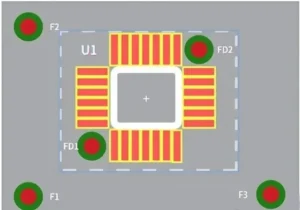
3. Process Edge Marker Points
Function: Used on panel assemblies to assist in positioning all circuit functions and facilitate alignment.
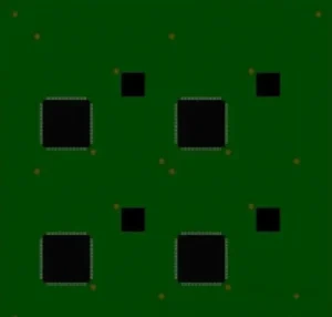
General Principles and Steps for Mark Point Positioning
1. Mark Point Shape
After selecting the reference mark positions, you can determine their display format.
While programmers design some manufacturing equipment to recognize various shapes—such as diamonds, squares, or hourglass shapes—not all machines can handle them.
It is still recommended to use the more universal circular mark points.
Why are circular mark points typically used?
- Circular objects are easier for machines to locate.
- For HAL completion, a convex shape on a circular reference point will remain circular, whereas on a square reference point, for example, it may no longer be square.
- Machines find it easier to locate the center of a circle.
- Circles have the smallest surface area.
- Circular shapes are uniformly etched.
- Multiple reference points can be used instead of inefficient odd-shaped ones, which theoretically might contain rotational information but are difficult to process.
- This feature differs most significantly from traditional circuit boards, which are predominantly rectangular.
- Circular mounting holes can double as inexpensive reference points.
Machine vision requires accurately locating reference points and then estimating their precise centers, with circular shapes being optimal.

2. Marking Dimensions
Reference marks may vary in size, primarily determined by the assembly machine.
Dimensions of 3.2mm solder mask aperture diameter with 1.6mm bare copper diameter, or 2mm solder mask aperture diameter with 1mm bare copper diameter, are generally compatible with all machines.
Reference mark dimensions on the same printed circuit board should not exceed 25 µm.We recommend making the minimum gap area twice the radius of the center mark.
A clear area should surround the reference point, free of any other circuit components or markings. The minimum size of this clear area should be twice the radius of the reference point.

PCB reference dimensions typically range from 1 to 3 millimeters, primarily determined by the assembly machinery used by the manufacturer.
Some manufacturers recommend adding three reference points at the corners of the circuit board, as this provides two angular alignment measurements and allows the pick-and-place machine to infer the correct orientation.
Certain manufacturers may specify the dimensions, depending on the assembly equipment they use.
Generally, the diameter of solder mask openings should be twice that of the reference bare copper diameter.
Additionally, PCB reference dimensions on the same board (both global and local) should be consistent, with variations not exceeding ~25 microns.
When assembling a 2-layer board, you should position the top and bottom reference points directly above each other.
The PCB reference dimensions for both the top and bottom layers should be identical, including solder mask openings.
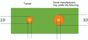
Local reference points are often as small as 1 millimeter, with solder mask openings of 2 millimeters.
Here is an active-voice revision:
Some manufacturers prefer the D-3D rule shown in the figure above because they favor larger solder mask openings.
Local PCB reference dimensions typically do not exceed 1 mm to accommodate trace routing and leave space for other components.
For very small components like 0201 resistors or chip-sized BGAs, the placement machine will be sufficiently precise, eliminating the need for local references.
The machine will accurately know where your components need to be placed.
3. Reference Point Edge Distance
Avoid placing reference points adjacent to the PCB edge. Assembly machinery typically uses fixtures to secure PCBs in position during assembly.
If fixtures cover reference points, serious issues arise. Position reference marks centrally at least 3 mm from the edge (5 mm is recommended to eliminate these risks).

4. Marker Point Composition
A marker point consists of three parts:
- A solid copper ring on the top or bottom copper layer
- A circle within the solder mask that serves as our alignment target
- An optional text label on the side

5. Marker Position Layout
You must establish multi-point surface alignment at the four corners or along the diagonals of the PCBA to ensure precise positioning with the maximum possible distance between markers.
1) PCB Marker Points
The placement machine’s PCB conveyance method determines where you place the markers.
When using rail conveyance, you must avoid placing markers near the gripping surface or alignment holes.
Specific dimensions depend on the placement machine model. The general requirements are illustrated below.
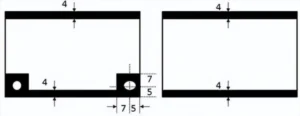
- During the positioning pin process, the mark points cannot be located.
- During edge alignment, the mark points cannot be positioned within 4mm of the edge to edge. PCB mark points should be placed along the diagonal, and the distance between them should be as large as possible.
- For PCBs shorter than 200mm, place at least 2 mark points as shown below. For PCBs longer than 200mm, place 4 mark points as shown in Figure b, with 1 or 2 mark points positioned along or near the centerline of the PCB’s long edge.
Place PCB mark points along the diagonal of each sub-board, as illustrated below.

2) Local Mark Points
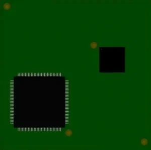
Position local mark points as follows: For QFP components with more than 100 pins, place 2 mark points along the diagonal, as shown in Figure a.
For QFP components with over 160 pins, place 4 mark points at the four corners, as shown in Figure b.

6. Mark Point Clearance
Adequate clearance around the mark point is critical. Leave an open area around the pad (free of copper, solder mask, silkscreen, etc.).
This space allows the camera to pick up the mark without visual interference.
The diameter of the open space should be at least twice the size of the pad. Therefore, for a 2mm pad, you need to leave at least a 4mm gap area around it.
The shape of the gap area is less important; circular and square areas are two popular designs.

7. Marking Points Material
Use the same metal as the rest of the circuit board to complete marking points and pads. (Remember, pads reflect light.)
Therefore, do not cover pads with solder mask, silkscreen, or any other material.
8. Number of Markers
Three reference points provide the optimal number for eliminating unexpected misalignment of the template relative to the PCB.
1) 1 Marker
With only one reference marker available, the scanning software cannot determine the correct rotation of the PCB. A machine cannot actually process a PCB with only one reference marker.
2) 2 Markers
With two reference markers available, the machine can operate normally. However, two risks come into play here.
- Dual-mark setup provides good but not always perfect position tracking. Accuracy may suffer with fine-pitch components.
- Opposite mark placement can lead to operator errors. If the PCB is inserted upside down, the machine may still detect the marks and proceed with its work. At best, this wastes time; at worst, it causes catastrophic component pile-ups or permanent damage to the PCB and equipment.
3) 3 Reference Points
Three is the optimal number of reference marks for proper PCB operation. Including a third reference mark adds an extra point for triangulation, thereby improving overall accuracy.
It also eliminates any possibility of incorrectly rotated boards passing through the camera.
4) 4 reference points
Although adding a fourth point might seem to improve accuracy, it provides little additional benefit.
The primary drawback here is that the fourth reference mark reintroduces the risk of processing upside-down panels. Exercise extreme caution when pursuing this approach.
9. Marking Copper Plating Surfaces
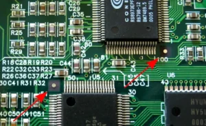
Ensure marking pads are smooth to reflect a uniform image. You can plate copper markings with any metal finish you choose.
Processes like electroplating and immersion plating are reliable for uniformity, whereas hot-air soldering often yields greater variation.

Any variation in the finish thickness will prevent accurate reflection. Although not insurmountable, it forces production operators to spend extra time restoring the markings.
Depending on the severity of the issue, it may require editing the software program to compensate or completely re-soldering the reference points. In short, the repair process is highly time-consuming.
10. Mark Point Contrast
You achieve optimal performance when the mark point contrasts strongly with the printed circuit board substrate. Ensure the internal background is uniform for all mark points.
Marking Point Creation
Component holes for interface devices and connectors are predominantly through-hole components.
The diameter of the through-hole is 8 to 20 mil larger than the pin diameter, ensuring good solder penetration during assembly.
Note that PCB holes may exhibit dimensional tolerances at the factory, typically within ±0.05mm.
Each 0.05mm corresponds to one drill size. For diameters exceeding 3.20mm, each 0.1mm corresponds to one drill size.
Therefore, when designing component hole diameters, convert units to millimeters and specify hole diameters as integer multiples of 0.05mm.
Manufacturers set drill tool dimensions based on user-provided drilling data. Drill tool sizes are typically 0.1–0.15mm larger than the user-requested finished hole diameter. The smaller the difference, the better.
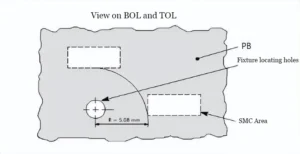
MARK Point Design Flaw Examples
Conclusion
Effective use of PCB reference points is key to maintaining assembly accuracy and consistency in automated electronics manufacturing.
Circular, well-sized, and properly cleared mark points—optimally three per board—allow placement machines to triangulate positions, prevent misalignment, and ensure correct component orientation.
Attention to materials, contrast, and positioning further enhances machine vision recognition and assembly reliability.
By following best practices in mark point design and layout, manufacturers can significantly reduce errors, improve production speed, and achieve superior PCB quality.

