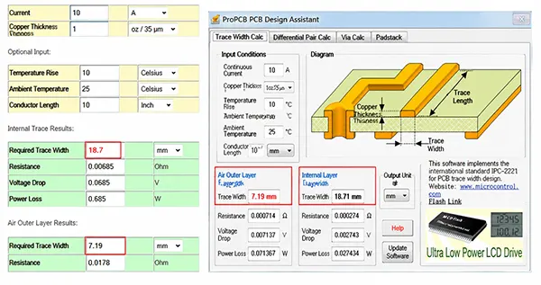
PCB Trace Width Calculation: How to Size Traces for High-Current PCB Designs
Learn how to calculate PCB trace width for high-current applications using the IPC-2221 standard. Discover how copper thickness, temperature rise, and current affect PCB trace sizing for reliable circuit board design.