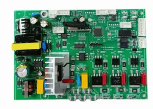
Safety spacing is a fundamental aspect of PCB design, especially for beginners who often encounter issues related to trace spacing, pad clearance, and mechanical interference.
Proper clearance not only ensures electrical reliability but also determines whether a design can be manufactured, assembled, and tested successfully.
This article introduces key electrical and non-electrical clearance rules in PCB design, helping designers avoid common pitfalls and improve overall board quality and manufacturability.
PCB beginners often encounter various pitfalls when starting, such as common spacing issues: the distance between traces, the distance between pads, and so on.
This article will discuss the topic of safety spacing in PCB design.

Electrical Clearance
1. Spacing Between Conductors
This spacing must account for the PCB manufacturer’s production capabilities. It is recommended that the minimum spacing between traces be no less than 4 mil.
This minimum trace spacing applies to both trace-to-trace and trace-to-pad distances.
From a production perspective, larger spacing is preferable whenever feasible. A standard 10 mil spacing is commonly used.
2. Pad Hole Diameter and Pad Width
Depending on the PCB manufacturer, the minimum pad hole diameter for mechanical drilling should not be less than 0.2mm. For laser drilling, a minimum of 4mil is recommended.
Hole diameter tolerance varies slightly by substrate material but is generally controlled within 0.05mm. The minimum pad width should not be less than 0.2mm.
3. Pad-to-Pad Spacing
Based on PCB manufacturer capabilities, a minimum spacing of 0.2mm between pads is recommended.
4. Copper Layer to Board Edge Spacing
For live copper layers, a minimum spacing of 0.3mm from the PCB board edge is preferred.
For large copper pours, an indentation distance from the board edge is typically required, generally set at 20mil.
Non-Electrical Clearance
1. Character Width, Height, and Spacing
For silk-screened characters, standard values such as 5/30 mil or 6/36 mil are typically used. Smaller text may appear blurred during printing.
2. Distance Between Silk Screen and Pad
Silk screen printing must not overlay pads. If silk screen covers a pad, solder cannot adhere to that area during soldering, compromising component placement.
Manufacturers typically require an 8 mil clearance. For extremely dense PCB layouts, a 4 mil clearance may be minimally acceptable.
If silkscreen inadvertently overlaps pads during design, manufacturers will automatically remove the silkscreen from the pad area during production to ensure proper solder wetting.
This requires careful attention.
3. Mechanical Structure
3D Height and Horizontal Clearance During component placement, consider potential conflicts with other mechanical structures both horizontally and vertically.
Design must fully account for spatial compatibility between components and between the finished PCB and the product enclosure, reserving adequate clearance for all target objects.

Partial Safety Clearance Rules
1). Clearance settings for high-voltage networks must comply with -48V power input port specifications:
Creepage distance and electrical clearance between the -48V power supply and all circuits except PGND must exceed 2.0mm;
Creepage distance and electrical clearance between PGND and other circuits must exceed 2.0mm.
2) Recommended PCB fabrication line width/spacing: 6mil/6mil; Minimum usable line width/spacing: 4mil/5mil; Absolute minimum line width/spacing: 4mil/4mil.
3) Solder mask bridges must be no less than 2mil (except for densely packed surface-mount devices like QFP packages), otherwise solder bridging between pads may occur during processing.
Recommended hole rules are as follows: ICT test via holes (32MIL pads) must maintain spacing no less than the following settings relative to pins, test pins, test vias, and thru pins:

1. Test Point Spacing Requirements
a) Center-to-center distance d between two test points: 85 mil preferred; 70 mil acceptable; 50 mil should be avoided.
b) Distance d from test point to via: 20 mil preferred; minimum 12 mil.
c) Distance d from test point to edge of bottom-side component pad: 20 mil preferred; minimum 12 mil. For single-board components undergoing wave soldering, 40 mil preferred; minimum 25 mil.
d) Test point to solder pad trace spacing d: 20 mil preferred; 12 mil minimum.
e) Test point to PCB edge spacing d: 125 mil minimum. Required only for O-ring fixtures.
f) Test point to locating hole spacing d: 200 mil preferred; 125 mil minimum. To facilitate locating pin installation.
The spacing between Thru pins, SMD pins, and test pins must not be less than the following settings and must also meet SMD component layout requirements, THD layout requirements, and crimped component layout requirements.

Conclusion
Adhering to well-defined PCB safety clearance guidelines is essential for achieving stable electrical performance, reliable soldering, and smooth manufacturing processes.
From conductor spacing and pad dimensions to silkscreen clearance, mechanical spacing, and test point layout, each rule plays a critical role in preventing short circuits, solder defects, and assembly conflicts.
By applying these clearance standards early in the design stage, PCB designers—especially beginners—can significantly reduce errors, enhance product reliability, and ensure efficient production and testing of their circuit boards.