PCB Design Guidelines: Layout, Routing & Thermal Relief Best Practices
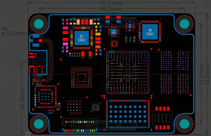
Essential PCB design guidelines for manufacturable boards. Learn component placement, signal routing, thermal relief pads, and DRC checks to avoid manufacturing defects.
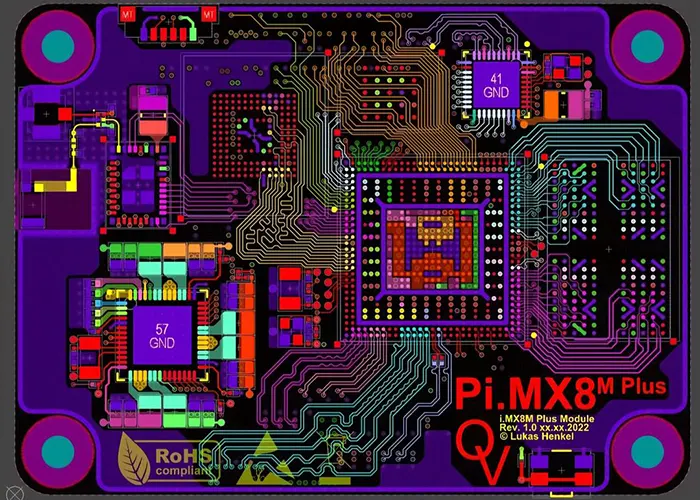
Master PCB routing with this comprehensive guide covering ground sharing, via design, power/ground line optimization, and DRC to achieve high-quality circuit board designs.
Master mixed PCB layout with these 9 essential tips covering component placement, analog-digital separation, grounding strategies, decoupling, PCB layering, copper resistance, and EMI shielding.
Learn the 7 most important PCB Routing principles for high-speed PCB design. Discover how proper power routing, impedance control, differential pair routing, length matching, trace spacing, and stub management improve signal integrity, reduce EMI, and enhance overall PCB performance.
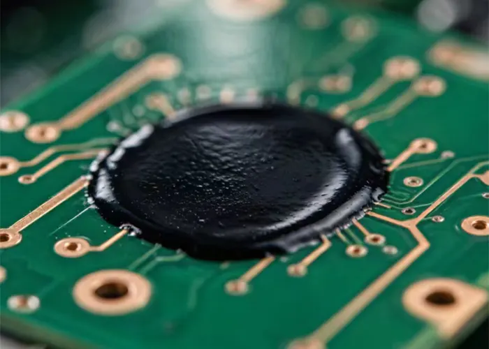
Printed circuit board (PCB) ink is an indispensable key material
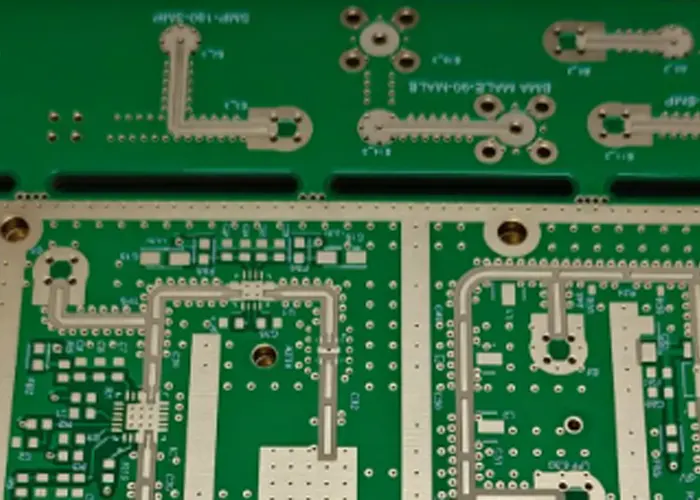
Millimeter-wave (mmWave) PCBs generally refer to circuit boards operating at frequencies in the 24 GHz, 28 GHz, 39 GHz, 60 GHz, 77 GHz, 79 GHz, or even higher bands.
PCB soldering quality is not determined by a single process step, but by the coordinated control of design, materials, equipment, and human operation throughout the entire manufacturing flow.
PCB beginners often encounter various pitfalls when starting out, such as common spacing issues: the distance between traces, the distance between pads, and so on. This article will discuss the topic of safety spacing in PCB design.
Numerous empirical formulas, correlation tables, and software tools regarding PCB trace width and current are available online. The following summarizes eight different formulas, tables, and calculation methods for the relationship between current and trace width.