In the era of deep integration between mobile internet and smart devices, smartphones have become the core equipment for daily life and work for users worldwide.
With the full commercialization of 5G technology, widespread application of artificial intelligence, and continuous upgrades in imaging and gaming capabilities, smartphones are rapidly evolving toward thinner designs, higher performance, and multifunctional integration.
This presents unprecedented challenges for the “nerve center” of smartphones—printed circuit boards (PCBs).
High-density interconnect (HDI) PCBs, with their high routing density, superior signal transmission performance, and strong spatial integration capabilities, have become the key components enabling breakthroughs in smartphone technology.
Traditional PCB technologies struggle to meet the increasingly complex functional demands of smartphones, revealing limitations such as insufficient routing, poor signal integrity, and inefficient interlayer interconnections.
As an advanced circuit technology, HDI boards significantly enhance circuit integration, shorten signal paths, and reduce electromagnetic interference through more precise layout techniques and laser microvia processing.
This makes them a critical enabling technology for smartphone development.
This paper investigates key technologies—thin core board fabrication, alignment accuracy, and precision patterning—using a 12-layer, 6-level arbitrary layer interconnection HDI board as a case study.
It aims to provide valuable insights for manufacturing high-end circuit boards for smartphones.
Experimental Section
Product Structure
This product is a 12-layer, 6-level HDI circuit board featuring an arbitrary-layer interconnect design.
The analysis discusses technical challenges encountered in the manufacturing process, including thin core board fabrication, alignment accuracy for high-order blind and via-through holes, precision pattern formation, and lamination parameters, while proposing corresponding solutions.
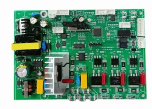
Figure 1 illustrates the product’s lamination structure, with key parameters listed in Table 1.

| No. | Item | Layer | Size (mm) | Spacing (mm) |
|---|---|---|---|---|
| 1 | Hole Diameter | L1–L12 | Hole: 0.085 | RING: 0.06 |
| 2 | Copper Thickness | L1–L12 | 0.02 | / |
| 3 | Minimum Line Width / Spacing | L1–L12 | Line width: 0.04 | Line spacing: 0.05 |
| 4 | Product Feature | – | 12-layer, 6-order Any-Layer Interconnect (HDI) | – |
| 5 | Finished Board Thickness | – | 0.8 mm | – |
| 6 | Panel Size | – | 618 × 723 mm | – |
| 7 | Surface Finish | – | Selective Gold Plating | – |
| 8 | Blind Via | – | 6-order stacked blind vias, any-layer interconnection | – |
| 9 | Application Field | – | Smartphones | – |
Table 1. Main Product Parameters
Manufacturing Process Flow
This 12-layer, 6-level HDI product for smartphone circuit boards requires six laser drilling operations, via plating, precision patterning, and five lamination processes. involving over 100 processes.
It poses significant challenges in material pressure resistance, drilling, pattern misalignment, and finished product reliability.
Key technical difficulties include the fabrication of thin core boards, laser drilling, plated through-hole plating, pattern alignment, blind/via alignment, precision circuit formation, and maintaining impedance consistency.
The specific process flow is as follows:
L6-L7: Material cutting → Baking → Laser positioning hole drilling → Passivation → Laser drilling → Plasma treatment → Passivation removal → Blind hole AOI → Electroplating → Via filling plating → Inner layer patterning → Inner layer etching → Line width measurement → Sub-outer layer AOI → Passivation
Secondary Outer Layer: Laminate → Target Hole Drilling → LDD Browning → Laser Drilling → Plasma Treatment → Browning Removal → Blind Hole AOI → Inner Layer Copper Plating → Full Board Via Filling Plating → Wafer Analysis → Secondary Outer Layer Pattern Formation → Secondary Outer Layer Etching → Line Width Measurement → Secondary Outer Layer AOI → Browning
Outer Layer: Laminate → Target hole drilling → LDD burn-in → Laser drilling → Outer layer drilling → High-pressure washing → Plasma treatment → Burn-in removal → Blind hole AOI → Outer layer copper plating → Whole board via filling plating → Wafer analysis → Outer layer pattern → Outer layer vacuum etching → Impedance test → HCT test → Outer layer AOI → Solder mask screen printing → Character screen printing → Solder mask Testing → Reflow Soldering → Sandblasting → Silk Screen Anti-Corrosion Gold Ink → Nickel-Gold Plating → Film Removal Electrolysis → Testing → 4-Wire Testing → Forming → Board Flex Check → Hole Inspection → Anti-Oxidation → FQC → FQA → Packaging
Production Control Challenges
Through data analysis and risk assessment, the following key production control challenges were identified based on the factory’s manufacturing processes:
(1) Core board thickness of 56 μm: Conventional fabrication often causes board jamming.
Laser-processed holes may retain adhesive residue at the bottom, compromising product reliability.
Electroplating often results in wrinkling, which impacts yield rates.
(2) The product undergoes 5 lamination steps and 6 laser drilling operations, making it difficult to control laser alignment accuracy and the reliability of laser hole stacking;
(3) Mobile phone products feature high wiring density, making pattern fabrication challenging.
(4) The 6-layer arbitrary interconnection product demands high reliability for blind vias.
Results and Discussion
Thin Core Board Fabrication
This product features an arbitrary interconnection design, requiring laser microvia technology to connect any layer from the core board to the outer layers.
The core board layer in mobile phone products is exceptionally thin, measuring only 56 μm thick.
Each production process step carries a high risk of board rejection, demanding stringent process control and design.
Additionally, the via-plating process for thin boards severely tests equipment capabilities.
Key Manufacturing Bottlenecks in Thin Core Boards
The critical bottlenecks in thin-core board fabrication are as follows:
(1) Laser direct drilling of the core board demands high-quality hole bottoms;
(2) Plasma stripping effectiveness on thin boards directly impacts final product reliability;
(3) Plating during via filling on thin boards is prone to wrinkling and poor fill coverage, affecting subsequent laser stacking.
(4) Pattern formation on thin boards presents significant challenges.
Process Optimization Strategies
To address these core board manufacturing bottlenecks, the following optimization solutions are proposed:
(1) Laser Drilling Process Optimization
Employing 18 μm thick copper foil paired with RTF copper foil significantly improves laser hole bottom quality.
Laser process testing optimizes laser parameters (see Table 2).
These laser parameters represent optimal results from extensive testing.
Actual production requires adjustments based on specific conditions.
Additionally, ensure top and bottom aperture measurements ≥90%, verify blind hole apertures, inspect hole bottoms, and prevent laser penetration through the bottom copper layer.
| No. | Hole Diameter | Pulse Width (us) | Energy (mj) | Shots (shot) | Aperture (mm) |
|---|---|---|---|---|---|
| 1 (Original Parameters) | 85 | 14 | 13 | 1 | 2.0 |
| 4 | 7 | 2 | |||
| 3 | 5 | 3 | |||
| 2 (After Optimization) | 85 | 13 | 12 | 1 | 2.0 |
| 4 | 6 | 2 | |||
| 3 | 5 | 3 |
Table 2. Core Board Laser Parameters
(2) Plasma Desmear Process Optimization
After laser drilling, plasma gas was used for de-gumming, while simultaneously testing the plasma de-gumming parameters and de-gumming effectiveness. See Table 3 for details.
| No. | Temperature (°C) | Desmear Time (min) | Power (W) | Gas Flow Rate (cc/min) |
|---|---|---|---|---|
| 1 (Original Parameters) | 80 | 25 | 8000 | 240 |
| 2 (After Optimization) | 80 | 30 | 8000 | 360 |
Table 3. Plasma Parameters
The stripping rate must be calculated using a stripping rate test piece.
Thin core boards require auxiliary tools for plasma stripping to prevent wrinkling during operation, which could affect pattern formation.
After plasma stripping, the passivation layer must be removed, and the blind via bottoms must be inspected using AOI equipment.
(3) Electroplating Process Optimization for Thin Boards
Due to the absence of horizontal plating lines in the current factory, conventional vertical plating lines may cause wrinkles due to insufficient fixture clamping force.
Product oscillation during fabrication leads to uneven copper plating thickness.
A double-sided clamping plating fixture must be used, securing the product from both top and bottom to prevent oscillation and wrinkling of thin boards during production.
Additionally, dual-side clamping enables electrical conductivity through both upper and lower surfaces, ensuring uniform board thickness.
Refer to Figure 2 for the fixture diagram.

Testing has confirmed that using double-sided clamping electroplating fixtures effectively prevents thin board wrinkling, ensures good copper thickness uniformity, and achieves near-100% via hole fill saturation, meeting product specifications.
(4) Pattern Formation Technology for Ultra-Thin Core Boards
With a core board thickness of 57 μm, conventional in-house dry film lamination for pattern formation often leads to poor film adhesion and low etching yield.
For thin-core boards, the production line focuses on inner-layer pattern processes.
Following standard inner-layer core board manufacturing procedures, wet film replaces dry film for pattern formation.
The wet film utilizes high-resolution liquid photosensitive ink with 35 μm resolution, and the post-application film thickness uniformity meets requirements.
In actual production, the wet film’s excellent filling properties enable precision pattern fabrication.
Combined with a high-precision LDI exposure system, it meets the requirements for line width/spacing of 40/50 μm.
Alignment and Testing Module
Mobile phone products and any interconnected devices inevitably feature small apertures, small pads, and dense circuit designs, which demand higher alignment precision.
The conventional approach involves using drill targets for positioning, laser-engraved drill targets for fabrication, and pattern-based laser target alignment.
As laser passes increase, cumulative misalignment in this method becomes more severe, potentially causing misaligned holes and damage.
This can lead to laser misconnections and short circuits in finished products, posing significant quality risks.
An illustration of blind hole misalignment is shown in Figure 3.

An analysis of the misalignment error in drill target positioning is conducted, with the drill target alignment process illustrated in Figure 4.

From the drill target alignment process perspective, laser alignment is used for drill targets, while laser ring targets are employed for outer layer pattern alignment.
Relative errors exist between these two alignment systems, causing misalignment among the final laser micro-holes, inner layer patterns, and outer layer patterns.
To address this issue, an optimization solution is proposed: uniformly adopt inner-layer target point alignment.
The drill target is solely used to locate the inner layer target points, which are then laser-etched.
Both laser processing and pattern alignment will utilize the inner layer target points.
The optimized process is illustrated in Figure 5.

To further enhance alignment accuracy, multiple inspection modules must be added.
During actual production, the alignment status of these inspection modules ensures that the finished product meets alignment requirements.
1. Laser Alignment Inspection Module
Due to stringent alignment requirements for blind holes in finished products, missed connections often only become apparent during electrical testing.
During laser drilling, the laser alignment inspection module monitors laser alignment status.
Any anomalies are promptly adjusted to prevent losses caused by undetected misalignment after laser drilling.
The laser alignment module is designed with the smallest hole ring on the board.
During laser drilling, the alignment module’s laser holes are created first, and the alignment of the hole bottoms is confirmed under a microscope.
Module Design Concept: Position the smallest through-hole ring as Position 3.
Gradually tighten the design for Positions 2 and 1, placing them around the perimeter and center of the working board.
During laser first-article inspection, examine the laser hole positions under a microscope for any substrate exposure.
Ensure no substrate exposure occurs at Position 3.
Capture and save a screenshot. The module diagram is shown in Figure 6.

Both the first and last parts in laser drilling must verify alignment with the alignment module to prevent blind holes from being missed.
Additionally, laser drilling requires tightening alignment to 95% of the specified alignment value.
2. Finished Blind Hole Alignment Module
The blind hole alignment module, also known as the resonance test module, facilitates finished product measurement to verify each laser alignment.
Through layer-by-layer stacking with progressively tighter tolerances, the module determines the range of blind hole misalignment.
It features three alignment points spaced at: PAD-20 μm, PAD-10 μm, and PAD.
By gradually tightening tolerances, it measures laser blind hole alignment during electrical testing.
The blind hole alignment module is illustrated in Figure 7.

Through the blind hole alignment module, the finished product measures blind hole loudness to verify alignment accuracy, ensuring that blind hole alignment meets requirements and that the overall alignment of high-order stacked holes complies with specifications.
The finished product cross-section is shown in Figure 8.

3. High Current Test Module (HCT Test)
A high-current test module within the PNL evaluates blind via reliability.
High Current Test involves designing a continuous chain of holes within the current board.
The module’s inherent resistance converts electrical energy flowing through the hole chain into thermal energy, generating tensile forces in different directions.
During testing, the temperature rises from room temperature to 220–260°C within one minute.
If defects exist in the plating integrity of blind holes or the bonding between plated copper layers, the equipment will trigger an alarm.
Failure analysis then confirms the blind via reliability. Figure 9 shows the HCT test module design.

Through the Full Test HCT module, efficiently verify blind via reliability.
Combined with finished product reliability testing, this approach prevents reliability risks associated with abnormal blind via bonding.
Precision Pattern Fabrication
The production of mobile phone products inevitably involves precision pattern fabrication.
This product features line widths/spacing of 40/50 μm. During manufacturing, improvements target precision pattern fabrication.
They focus on equipment selection, line resolution, etching uniformity, copper plating thickness uniformity, and dynamic line compensation.
(1) A 25 μm thick dry film, combined with a high-precision LDI exposure system, achieves excellent resolution for precision circuits.
Post-development measurements confirm that both line width and spacing meet specifications.
Vacuum etching combined with two-fluid line etching performs the etching.
Vacuum etching effectively prevents pooling effects, while two-fluid etching enhances the etch factor.
Line width measurements consistently fall within tolerances, satisfying customer requirements.
(2) Using laser-burned inner layer targets for alignment on each layer minimizes alignment deviation and reduces cumulative errors.
(3) Before pattern formation, CMI full copper thickness measurement was performed, with 9 points measured on each wafer (top, middle, bottom) to ensure copper thickness of 20±3 μm.
(4) Dynamic compensation ensures line width consistency.
Different compensation values correspond to varying spacings, line width types, and pads, as shown in Figure 10.
Through these improvements, all line widths fall within the required range, meeting the demands of precision circuit fabrication.
Test Results
To verify product reliability, the product underwent reliability testing, including thermal shock, pad pull-off, blind hole pull-off, dielectric strength, and thermal cycling tests.
All test results were satisfactory.

Conclusion
High-density interconnect (HDI) circuit boards for smartphones serve not only as their physical carriers but also as critical components ensuring smartphone performance and reliability.
This paper analyzes key technologies for smartphone HDI circuit boards, covering chip-on-board fabrication, alignment accuracy, precision patterning, and finished product reliability.
Corresponding optimization solutions address the identified challenges.
Following these optimized procedures, the overall yield meets requirements, and the product has passed customer validation.