
Mixed-signal PCB design is one of the most challenging tasks in hardware engineering, where sensitive analog circuits and noisy digital components share the same board.
Poor layout can lead to signal interference, ground noise, and degraded performance—problems that are often difficult to diagnose and fix after manufacturing.
This guide presents nine practical tips for mixed PCB layout, covering everything from component placement and analog-digital separation to grounding strategies, decoupling techniques, and EMI shielding.
Whether you’re designing a data acquisition system or a complex mixed-signal device, these principles will help you achieve clean, reliable circuit performance.
Component Placement
When placing components, follow the signal paths shown in the schematic and allow sufficient space for routing.
In addition, follow these placement rules:
Designers should place power supply components close together and decouple them properly to ensure power integrity.
Place decoupling capacitors as close as possible to the associated components to reduce parasitic inductance and ensure stable operation.
Designers should place connectors at the edge of the board.
Follow the schematic guidelines for high-frequency components.
Designers should place large memory devices and processors, such as clock generators and controllers, in the center of the circuit board.
Separation of Analog and Digital Modules
Designers aim to minimize shared return paths for analog and digital signals.
For this purpose, they separate analog and digital modules.
This layout method prevents analog signals and digital signals from mixing.
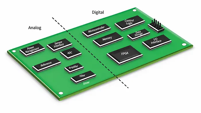
The figure above shows an example of separating analog and digital circuits.
When dividing the circuit into analog and digital sections, keep the following points in mind:
It is recommended to place precision analog components, such as amplifiers and reference voltage sources, on the analog plane.
The opposite side serves as the digital plane. Designers must reserve this area for noisy digital components.
Typical examples include logic control units and timing blocks.
Systems contain analog-to-digital converters (ADCs) and digital-to-analog converters (DACs).
These devices belong to mixed-signal components. They carry relatively low digital currents.
Designers should handle them the same way as analog components in an analog system.
For designs with a large number of high-current ADCs and DACs, it is recommended to separate the analog and digital power supplies.
In other words, designers connect DVDD to the digital section, while they route AVCC to the analog section.
Microprocessors and microcontrollers produce considerable electromagnetic radiation and heat.
Designers place these components at the center of the circuit board to boost heat dissipation.
They also position the components close to the circuit blocks they connect to.
Trace Routing
Designers place all components in their optimal positions. They also build a suitable ground plane.
Once they finish these two steps, most traces will naturally follow the correct path.
However, keep the following guidelines in mind when routing traces:
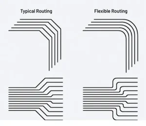
Signal paths should be as direct and short as possible.
Layers containing high-speed signal paths should have an adjacent ground layer to ensure proper signal return.
High-speed circuits are particularly sensitive and require that signal paths follow the layout specified in the schematic.
Minimize inductance in power traces by using short, direct, and wide traces.
Avoid creating antennas when routing traces and via holes.
Power traces should be short, compact, and use wide traces.
Routing must maintain isolation between digital and analog circuit components.
Grounding is critical, especially for traces connecting digital and analog partition areas.
Power Supply Modules
Power supplies play a critical role in circuits. Designers must handle these modules with care.
Designers usually place power supply modules close to the components they supply power to.
Meanwhile, they isolate these modules from other parts of the circuit.
Devices inside complex systems often have a large number of power pins.
Under this condition, designers can adopt dedicated power supply modules for analog and digital areas.
This measure prevents digital noise from causing interference.
Designers should route power traces short and straight and adopt wide traces to reduce inductance and avoid current limiting.
Decoupling
One of the key factors engineers must consider to meet a system’s performance requirements is the power supply rejection ratio (PSRR).
PSRR ultimately determines a device’s performance. This indicator measures how sensitive the device is to power supply fluctuations.
Designers need to maintain optimal PSRR. To achieve this target, they must stop high-frequency energy from entering the device.
To achieve this, a combination of electrolytic and ceramic capacitors can effectively isolate the device’s power supply from the high-impedance ground plane.
Effective decoupling ensures a low-noise environment during circuit operation.
The basic rule is to provide the shortest possible path to facilitate the return of current.
The following are some common decoupling methods:
Designers use low-inductance ceramic capacitors to suppress high-frequency noise.
They deploy electrolytic capacitors as charge reservoirs for transient currents to filter low-frequency noise on power supplies.
Additionally, ferrite beads are optional but can enhance isolation and decoupling from high-frequency noise.
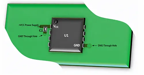
Designers should place decoupling capacitors as close as possible to the device’s power pins.
Designers connect these capacitors to the main region of the low-impedance ground plane through vias or short traces.
This arrangement minimizes extra series inductance.
Designers should position power pins close to the device body and select smaller capacitors, generally ranging from 0.01 μF to 0.1 μF.
This configuration prevents the device from operating erratically when multiple outputs switch simultaneously.
The distance between the electrolytic capacitor and the device’s power pins should not exceed one inch (typically 10 F to 100 F).
Designers want to simplify PCB layout work. They can connect decoupling capacitors to the ground plane with a T-connection.
They place vias near the device’s GND pin for this connection. This method lets designers avoid extra trace routing.
For specifics, see the figure below:
PCB Layering
Before routing a PCB, you must carefully consider its layer stackup; otherwise, it will affect the return paths allowed by the system design.
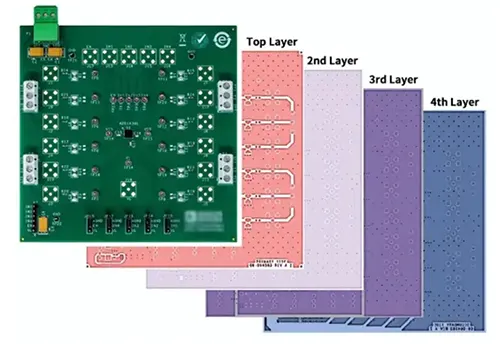
The figure above shows a visual representation of the various layers of a circuit board.
The figure below provides a detailed overview of a typical PCB layout:
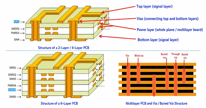
High-performance data acquisition systems typically consist of four or more layers.
Auxiliary signals are usually routed on the bottom layer, while digital and analog signals are typically routed on the top layer.
By serving as a reference layer for impedance-controlled signals, the second layer (also known as the ground plane) reduces IR voltage drops and protects the digital signals on the top layer.
The power supply layer is located on the third layer.
Designers place the power supply layer and the ground layer close to one another.
The two layers create extra interlayer capacitance, which ensures effective power supply decoupling under high-frequency conditions.
PCB Copper Resistance
Copper resistance is also important in mixed-signal PCB layout, as copper traces can form effective interconnects and ground planes.
Most PCBs use 1 oz of copper, but high-power sections may use 2 or 3 oz of copper. At 25°C, the resistivity of copper is 1.724 × 10⁻⁶ Ω/cm.
A common 1 oz copper foil thickness is 0.036 mm (0.0014 in), with a resistivity of 0.48 mΩ/sq.
For example, the resistance per unit length of a 0.25 mm (10 mil) wide trace commonly used on PCBs is approximately 19 mΩ/cm (48 mΩ/in).
PCB trace resistance can be a source of error for mixed-signal ICs.
For a 16-bit ADC with a 5 kΩ input resistance, driven by a 5 cm, 0.25 mm wide, 1 oz copper trace, the trace resistance is 0.1 Ω, and when combined with a 5 kΩ load to form a voltage divider, it produces an error of 0.1/5 k (approximately 0.0019%), which exceeds the 1 LSB (0.0015%) of a 16-bit ADC, as shown below:
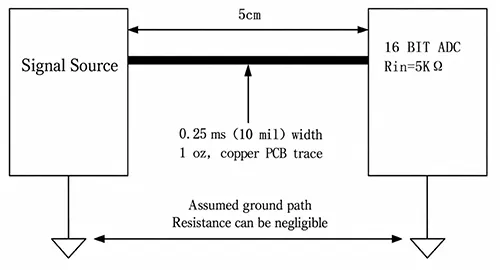
In practical applications, the situation may be even more severe, as this approach ignores the return path and copper’s temperature coefficient of 0.4%/°C at 25 °C.
When working with low-impedance precision circuits, copper resistance is critical to a successful design.
Grounding
Single Ground Plane
The best approach for mixed-signal systems with a single ADC or DAC handling low-amplitude currents is to use a single solid ground plane.
To understand the importance of a single ground plane, it is necessary to analyze return currents.
The term “return current” describes the current that completes the circuit loop and flows back to ground.
Each return path must be carefully routed throughout the PCB layout to avoid mixed-signal interference.
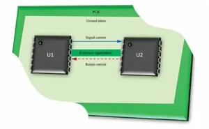
The simple circuit shown above illustrates the advantage of a single solid ground plane over multiple ground planes.
A return current equal in magnitude but opposite in direction to the signal current exists.
When the return current flows back to the source in the ground plane, it will take the path of least resistance.
The path of least resistance (typically a straight line between the equipment’s ground references) will be followed by the return current for low-frequency transmission.
However, a portion of the return current will attempt to return along the signal path for higher-frequency transmission.
This is because the impedance between the output and return currents along that path is lower and the loop is smaller.
Separate Analog and Digital Grounds
Another common strategy is to divide the ground plane into two sections: an analog ground plane and a digital ground plane.
This approach is suitable for more complex systems with a large number of mixed-signal components and high digital current requirements.
The figure below shows a schematic of a system with a divided ground plane.
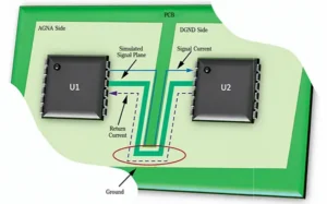
Eliminating breaks in the ground plane and allowing return current to take a more direct path back through a star ground connection is the simplest method for achieving a unified ground for systems with separate ground planes.
In mixed-signal layouts, the intersection of the analog and digital ground planes is referred to as a star ground.
A star ground can be connected to the typical thin, continuous connection between the analog and digital ground planes found in common systems.
For more complex systems, star grounding is typically implemented by routing jumpers to the ground connection.
Since no current flows through a star ground, high-current-carrying connectors and jumper splitters are not required.
The primary function of a star ground is to ensure that the reference levels of the two grounds are the same.
On the other hand, because star grounding also connects the two ground planes at a single point, mixed-signal devices with AGND and DGND pins can be connected to their respective ground planes.
This isolates precision analog circuits from high-noise digital currents, which flow through the digital power supply, reach the digital ground plane, and then return to the digital power supply.
Multilayer PCBs must achieve complete isolation between the AGND and DGND planes.
Electromagnetic Interference (EMI) Shielding
Even after addressing ground loops, crosstalk, power supply noise, and other forms of interference, a circuit may still be susceptible to electromagnetic interference (EMI).
This can lead to various problems, such as:
- Interference with wireless communications.
- Communication interruptions.
- Corrupted sensor data.
- Component failures.
- Software errors and malfunctions.
One effective method for addressing EMI is to use a sufficient amount of metal shielding.
Preferably, the shielding should form a Faraday cage that encloses the circuit on all six sides and connects to ground.
Although shielding can block most incoming EMI, it is also necessary to address thermal management and allow for signal input and output.
Conclusion
A successful mixed PCB layout relies on a systematic approach that balances signal integrity, power integrity, and noise control.
By following these nine tips—from strategic component placement and analog-digital separation to proper grounding, decoupling, and EMI shielding—you can significantly reduce interference and ensure reliable circuit performance.
Remember that there is no one-size-fits-all solution; the choice between a single ground plane and separate analog-digital grounds depends on your system’s complexity and current requirements.
Apply these principles thoughtfully to your next mixed-signal design, and you’ll see measurable improvements in noise reduction and overall circuit stability.

