
When engineers begin a new electronic design project, most working hours are usually devoted to circuit design and component selection.
This creates a common situation in the subsequent work. It happens at the PCB layout and routing stage.
Designers often lack sufficient relevant experience. They are unable to conduct comprehensive consideration of all influencing factors.
Failing to devote sufficient time and effort to the PCB layout and routing phase can lead to manufacturing issues or functional defects when the design transitions from the digital realm to the physical world.
So, what is the key to designing a circuit board that is reliable both on paper and in physical form?
Let’s explore the following six PCB design guidelines you need to understand when designing a manufacturable, functionally reliable PCB.
Fine-Tune Your Component Placement
The component placement stage of the PCB layout process is both a science and an art, requiring strategic consideration of the key components available on the circuit board.
This design process can present many challenges. The placement of electronic components carries great significance.
It directly affects the manufacturability of the circuit board.
Component layout also determines whether the board can satisfy the initial design requirements.
There exists a commonly adopted sequence for component placement. The typical order follows certain arrangements.
Designers place connectors and PCB mounting components first. Next come power circuits, precision circuits and critical circuits in turn.
Apart from this general sequence, several specific guidelines need to be followed. The main points are listed as follows:
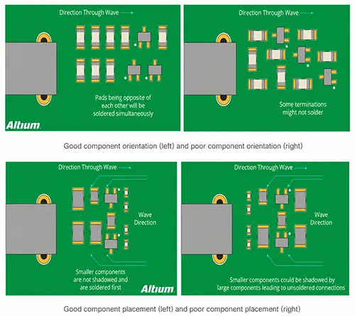
Orientation—Ensure that similar components are oriented in the same direction, which will help ensure an efficient and error-free soldering process.
Layout – Avoid placing smaller components behind larger ones, as the smaller components may be affected by the soldering of the larger ones, leading to placement issues.
Organization – It is recommended to place all surface-mount (SMT) components on the same side of the board and all through-hole (TH) components on the top of the board to minimize assembly steps.
Here is one last important guideline for PCB design. Designs may adopt mixed-technology components.
They include through-hole components and surface-mount components.
In this case, manufacturers need to adopt extra assembly processes. These additional working procedures will push up the total production cost.
Proper Placement of Power, Ground, and Signal Traces
After placing the components, you can proceed to place the power, ground, and signal traces to ensure your signals have a clean, interference-free path.
At this stage of the layout process, keep the following guidelines in mind:
Positioning Power and Ground Planes
It is always recommended to place the power and ground planes inside the circuit board, while maintaining symmetry and centering.
This helps prevent the circuit board from warping and ensures that your components are positioned correctly.
When powering ICs, it is recommended to use a common trace for each power supply, ensure a consistent and stable trace width, and avoid daisy-chaining power connections between components.
Signal Trace Routing
Next, route the signal traces according to the design in the schematic.
It is recommended to always use the shortest and most direct paths possible between components.
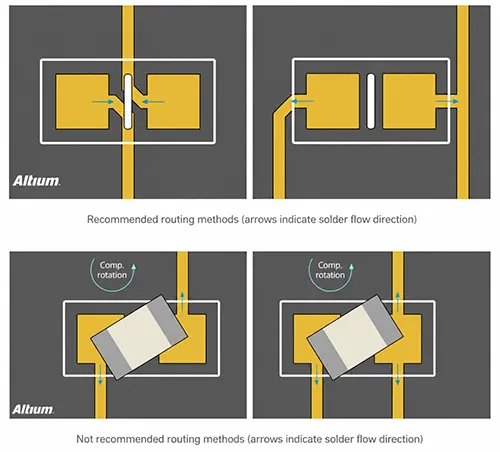
Components may require perfectly level positioning on the PCB. Under such circumstances, a recommended routing strategy can be adopted.
Conduct traces roughly horizontally at the component leads. Once the traces extend away from the leads, route them vertically.
This ensures that the components remain level as the solder flows during soldering, as shown in the upper half of the figure below.
In contrast, the signal routing method shown in the lower half of the figure below may cause the components to shift as the solder flows during soldering.
Defining Trace Width
Your design may require different traces that carry various currents, which will determine the required trace width.
With this basic requirement in mind, a width of 0.010’’ (10 mil) is recommended for low-current analog and digital signals.
When your trace current exceeds 0.3 amps, the trace should be widened. Here is a free trace width calculator to simplify this conversion process.
Effective Isolation
You may have experienced how high voltage and current spikes in power circuits can interfere with your low-voltage control circuits.
To minimize such interference issues, follow these guidelines:
Isolation—Ensure that the power ground and control ground are kept separate for each power supply.
If you must connect them on the PCB, make sure to do so as close as possible to the end of the power path.
This requirement belongs to PCB layout specifications. You may arrange a ground plane on an intermediate layer.
If you do so, one key measure must be implemented. It is necessary to create a low-impedance current path.
This path can lower interference risks originating from power circuits. Meanwhile, it offers effective protection for control signals.
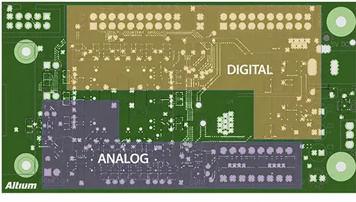
You can follow the same guidelines to keep your digital and analog circuits separate.
Coupling—To minimize capacitive coupling caused by large ground planes and traces routed above and below them, try to cross analog ground only via analog signal lines.
Solving Heat Problems
Have you ever experienced reduced circuit performance or even PCB damage due to heat issues?
Many designers have encountered problems because they failed to consider heat dissipation.
Here are some guidelines to keep in mind to help solve heat dissipation issues:
Identify Problem Components
The first step is to identify which components generate the most heat on the circuit board.
This can be done by first locating the “thermal resistance” rating in the component’s datasheet and then following the recommended guidelines to dissipate the generated heat.
Of course, heat sinks and cooling fans can be added to keep component temperatures down, and it’s also important to position critical components away from any high-heat sources.
Add Hot-Air Pads
Adding hot-air pads is very useful for producing manufacturable circuit boards;
They are essential for high-copper-content components and wave soldering applications on multilayer boards.
It is hard to stabilize the temperatures during the manufacturing process.
For this reason, hot-air pads are recommended for through-hole components.
These pads slow down heat dissipation at component leads. This measure can greatly simplify the soldering procedure.
As a general rule, always use hot-air pads for any through-hole or via connected to the ground plane or power plane.
In addition to hot-air pads, you can also add teardrops at the pad connection points to provide additional copper foil/metal support.
This will help reduce mechanical and thermal stress.

An Introduction to Hot-Air Solder Pads
Many factories have engineers in charge of manufacturing processes and SMT technology.
These engineers often come across various soldering defects. Typical defects include solder voids, de-wetting and cold solder joints.
These problems share a common characteristic. The solder fails to properly wet the components on the circuit board.
No matter how process conditions are adjusted or how reflow oven temperatures are fine-tuned, there is always a certain rate of non-wetting defects.
What exactly is causing this?
Setting aside issues related to component and PCB oxidation, a root cause analysis reveals that a significant portion of these soldering defects actually stems from flaws in the PCB layout design.
The most common issue is when certain component leads are connected to large areas of copper trace, causing these leads to fail during the reflow soldering process.
Some hand-soldered components may also experience cold solder joints or solder balls due to similar circumstances, and in some cases, components may even be damaged by excessive heating.
In PCB design, large areas of copper foil are often laid out to serve as power supplies (Vcc, Vdd, or Vss) and ground (GND).
These large copper foil areas are typically connected directly to the pins of control circuits (ICs) and electronic components.
Regrettably, large copper regions need to be heated up to solder melting temperature.
The heating process consumes more time than that of independent single pads. In other words, the heating speed is relatively slow.
In addition, heat dissipates at a faster rate on these copper areas.
Large-area copper foil traces have two ends. One end connects to small components like tiny resistors or capacitors.
The other end remains unconnected. In this layout condition, soldering problems tend to occur easily.
The root cause lies in inconsistent melting and solidification time of the solder.
The reflow soldering temperature profile may lack proper adjustment. In addition, the preheating duration could be inadequate.
In such cases, component leads connected to large copper foil areas face risks.
These leads cannot reach the melting temperature of solder. As a result, cold solder joints are likely to form.
During manual soldering (Hand Soldering), the leads of components connected to large areas of copper foil cannot be soldered within the specified time due to excessive heat dissipation.
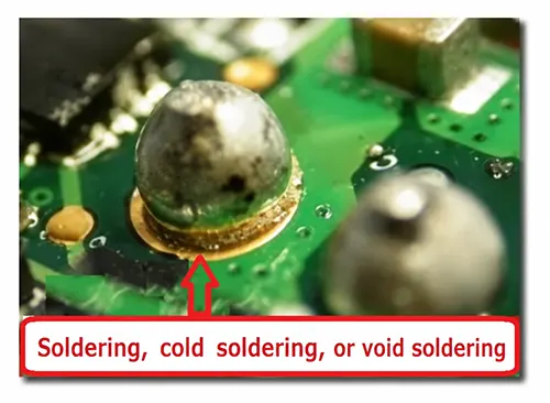
The most common defects are solder balls and cold solder joints, where the solder is attached only to the component lead and does not connect to the PCB pad.
From visual observation, the whole solder joint presents a spherical shape.
When the situation becomes more serious, operators will take countermeasures.
They may continuously raise the temperature of the soldering iron. Or they apply heat for an excessively long period.
Their goal is to weld the lead onto the PCB. However, this operation makes components surpass their thermal tolerance limit.
The components end up being damaged without the operators noticing.
As shown in the figure below.
Now that we’ve identified the problem, we can find a solution.
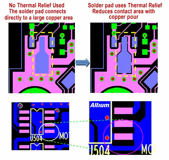
Generally, we recommend using a “thermal relief pad” design to address soldering issues caused by large areas of copper foil connecting to component leads.
As shown in the figure below, the layout on the left does not use thermal relief pads, while the layout on the right employs this connection method.
As you can see, the contact area between the pads and the large copper foil is limited to just a few thin lines.
This significantly restricts heat loss from the pads, resulting in optimal soldering performance.
Check Your Work
When you’re rushing to assemble all the parts for manufacturing, it’s easy to find yourself overwhelmed by problems that only surface at the end of the design project.
Therefore, double- and triple-checking your design work at this stage can mean the difference between a successful and a failed manufacturing run.
Quality control procedures need to be fully implemented. We always suggest carrying out two checks at the initial stage.
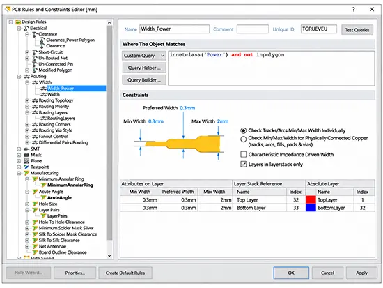
They are Electrical Rule Checks (ERC) and Design Rule Checks (DRC). These checks serve an important verification purpose.
They confirm whether the design meets all specified rules and constraints.
Using these two systems, you can easily check for spacing, trace width, common manufacturing settings, high-speed requirements, short circuits, and more.
When ERC and DRC produce results without any errors, we advise performing a detailed inspection of every signal routing.
The inspection covers the whole path from schematic to PCB. Check signal traces one line after another.
This method helps carefully confirm that no details are neglected.
Additionally, use the probe and mask features of your design tool to ensure that your PCB layout matches your schematic.
Conclusion
Every PCB designer ought to learn these design guidelines. After you fully master them, consistently follow these suggestions.
You will soon gain the capability to design high-performance circuit boards.
These boards are easy to manufacture. Ultimately, you can fabricate printed circuit boards with outstanding quality.
Good PCB design practices are essential for success, and these design rules lay the foundation for building and reinforcing a culture of continuous improvement across all design practices.

