
On a PCB, incorrect pad dimensions, alignment, or placement can lead to problems with component electrical performance and manufacturability.
Pads in PCB design are like the foundation of a house—if the foundation isn’t laid properly, can the house be stable?
Similarly, if there are problems with the PCB pad design, can the board be reliable?

What are Pads in PCB Design?
A pad is an exposed metal area on a circuit board used to connect the circuitry on the die to the pins of the packaged chip.

Problems Caused by Incorrect Pad Sizes on PCBs
The size, shape, and position of pads in a PCB package directly affect the manufacturability of the circuit board.
During the soldering process in PCB assembly, using pads with incorrect dimensions or improper placement can lead to various problems. The following are a few examples:
Floating Components
If a surface-mount component is placed on a pad that is too large or spaced incorrectly, the component may float out of position during reflow soldering.
This can cause solder bridging to other metal areas and result in insufficient component spacing during cooling, rework, and PCB testing.
Incomplete Solder Joints
Pads that are too small or spaced too closely together may not provide enough space to form adequate solder fillets.
This can result in poor solder connections or no solder joints at all.
Solder Bridging
Surface-mount pads that are too large can cause components to float, which may lead to solder bridging.
This occurs when solder flows across a pad or metal feature on another circuit, creating a direct short circuit.
Solder bridging can also occur if the correct solder mask and solder paste features are not designed into the pad shapes within the CAD tool.
Tombstoning
Soldering issues may arise with small, dual-lead SMT components, such as resistors and capacitors, if their pad sizes differ.
One pad will heat up faster than the other, and the molten solder will pull the component upward away from the other pad, causing it to stick to the pad like a tombstone.
Solder Capillary Action
Through-hole pads can also pose challenges if not designed correctly.
If the drill hole is too large for the component leads entering the hole, the solder may be drawn through the hole by capillary action before a good connection is established.
On the other hand, a drill hole that is too small makes it difficult to insert the component leads and slows down the assembly process.
Through-Hole Breakage
Through-hole pads must have a solid annulus to ensure solderability; this is the metal between the hole wall and the outer perimeter of the pad.
The annulus is designed to be large enough to accommodate the expected deviation of the drill bit from the center of the hole.
However, if the pad is too small, the annulus may develop cracks, and excessive cracking can lead to poor soldering or circuit damage and incompleteness.
If the pad size is too small for the drill bit being used, the drill bit may wobble slightly during normal drilling operations and deviate from the intended pad shape.
Short Circuits with Other Metals
Pads that are too small can cause surface traces to come too close to the components soldered onto them, creating potential areas for metal short circuits.
On the other hand, pads that are too large may restrict the routing of traces between them, making PCB routing more difficult.
Classification of Pad Designs in PCBs
Surface-Mount Pads
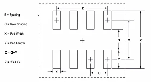
1) Pads used to mount surface-mount components are called surface-mount pads. These pads have the following characteristics:
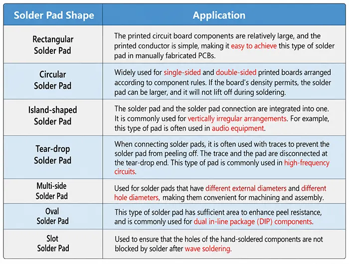
They are pads with a visible copper area. They can be rectangular, circular, square, or other shapes such as rectangles.
2) Solder mask
3) Solder paste
4) Pad count (number of pads on the component)
Through-Hole Pads
Pads used to mount through-hole components are called through-hole pads, and there are two types:
1. Plated Through-Hole (PTH)
PTH refers to pads with through-holes, where the hole walls are plated with copper and, in some cases, solder or other protective coatings.
The plating of the holes is accomplished using an electrolytic process, and the plating provides an electrical connection between the different layers of the circuit board.
2. Non-Plated Through-Hole (NPTH)
NPTH refers to pads where the holes are not plated. These pads are primarily used on single-sided boards or when the holes are used to mount the PCB into an enclosure, with screws inserted through them.
Typically, unplated holes have no copper in the area surrounding the hole (similar to the board edge clearance), which is done to prevent short circuits between the copper layer and the components to be placed.
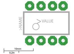
The different parts of a through-hole pad are commonly referred to as the pad stack and include: top pad, bottom pad, inner pad, drill, annulus, and PIN.
Special Features of BGA Pads
1. SMD Pads and NSMD Pads
Proper pad design is critical to ensuring the manufacturability of BGA components.
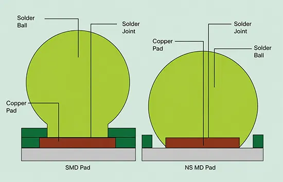
There are essentially two types of BGA pads—solder mask-defined pads (SMD) and non-solder mask-defined pads (NSMD).
2. Solder Mask-Defined (SMD) BGA Pads
SMD pads are defined by solder mask apertures applied to the BGA pads.
These pads feature solder mask apertures where the mask opening is smaller than the diameter of the pad they cover; this is done to reduce the size of the copper pad to which the component is soldered.
The figure below shows how to specify that the solder mask covers a portion of the copper pad beneath it.
This offers two advantages: first, the overlapping mask helps prevent the pad from lifting off the board due to mechanical or thermal stress.
The second advantage is that the opening in the mask creates a channel for each BGA ball, allowing it to align with the ball as the component passes through the soldering process.
The copper layer for SMD BGA pads typically has the same diameter as the pads on the BGA. To create the SMD mask, a 20% reduction is traditionally applied.
3. BGA Pads Not Defined by the Solder Mask (NSMD)
The difference between NSMD pads and SMD pads is that the solder mask is defined so that it does not contact the copper pads; a mask is created to produce a gap between the pad edges and the solder mask.
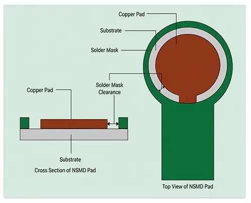
Here, the size of the copper pads is defined by the diameter of the copper pads rather than by the mask layer.
NSMD pads can be smaller than the diameter of the solder balls, with the pad size reduced by 20% of the solder ball diameter.
This approach leaves more space between adjacent pads, making routing easier, and is used for high-density and fine-pitch BGA chips.
One drawback of NSMD pads is that they are prone to delamination due to thermal and mechanical stresses.
However, delamination of NSMD pads can be prevented by following standard manufacturing and handling practices.
How Do You Determine PCB Pad Design Dimensions?
The following methods can be used to obtain the correct dimensions and shapes for the PCB pads and component packages you will be using.
Industry Standards
Over the years, the PCB design industry has established standards for various aspects of circuit board layout, including recommended pad and pad pattern dimensions.
IPC-7351 is one such standard, and there are other examples as well.
Pad and Pad Pattern Generators
Today’s Electronic Design Automation (EDA) tools include pad and pad pattern generators, also known as library wizards.
These software features are typically integrated with IPC standards and automatically generate the required pad shapes and dimensions for components.
Component Supplier Datasheets
Every PCB component manufacturer publishes a datasheet for the parts they offer.
In addition to the electrical and physical specifications in these datasheets, they typically include recommended PCB layout pad patterns.
Pad and Pad Pattern Calculators
Engineers and other users can find a variety of pad and pad pattern calculators online.
Company Standards
Many companies have their own pad and pad pattern standards, which they expect to be followed when designing circuit boards.
These standards are typically a combination of industry standards and supplier specifications tailored to specific PCB manufacturers.
PCB Design CAD Vendor Libraries
EDA tools also provide pre-built pad libraries and pad patterns that licensed users can download and use.
PCB Manufacturers
Individual contract PCB manufacturers may also have preferred PCB pad sizes and patterns that they want you to follow; they should be able to provide pad sizes and shapes that best suit their own manufacturing processes.
Third-Party Library Providers
There are also online PCB library providers that have created pad and pad pattern libraries and make them available for use.
However, standards should govern not only the size and shape of PCB pads but also the spacing required for precise component placement.
If components are placed too close together on the board, they may cause the same solder bridging issues as incorrectly sized pads.
Design Standards for Pad Shapes and Dimensions in PCB Design (For Reference Only)
1. The minimum single-sided dimension of all pads shall be no less than 0.25 mm, and the maximum diameter of the entire pad shall not exceed three times the component hole diameter.
2. Keep the spacing between the edges of two pads greater than 0.4 mm whenever possible.
3. Use oval or rectangular pads in areas with dense routing. Design single-sided pads with a diameter or minimum width of 1.6 mm, and use a hole diameter of 0.5 mm for double-sided pads in low-current circuits.
If pads are too large, they can easily result in unnecessary solder joints.
Design pads with a hole diameter exceeding 1.2 mm or a pad diameter exceeding 3.0 mm as diamond-shaped or flower-shaped pads.
4. For through-hole components, fully cover single-sided connection pads with copper foil to prevent copper foil damage during soldering.
however, for double-sided boards, the minimum requirement is to compensate for teardrop-shaped pads.
5. Design all machine-mounted components with drip pads along the bending direction to ensure complete solder joints at the bent leads.
6. Use daisy-chain pads instead of dummy pads on large copper pads.
If the PCB has large ground or power plane areas (exceeding 500 mm²), these areas should be partially open or designed with a grid fill pattern.
PCB Pad Design and Manufacturing Process Requirements (For Reference Only)
1. Place test pads at both ends of surface-mount components where they are not connected to through-hole components.
The diameter of the test pads should be equal to or greater than 1.8 mm to facilitate testing by in-line testers.
2. For IC pads with tight spacing that are not connected to through-hole pads, add a test pad.
For surface-mount ICs, do not place test pads within the IC’s silkscreen.
Test pad diameters should be equal to or greater than 1.8 mm to facilitate testing by in-line testers.
3. If the pad spacing is less than 0.4 mm, apply solder mask to reduce solder bridging.
4. Design the leads of surface-mount components with lead-tin joints.
Use a wire width of 0.5 mm for the lead-tin joints, with a typical length of 2–3 mm.
5. If a single-sided board contains hand-soldered components, a tin via must be provided. Its orientation should be opposite to that of the solder. The via width should be between 0.3 mm and 1.0 mm.
6. The spacing and dimensions of conductive adhesive buttons should match the actual dimensions of the buttons.
Conclusion
PCB pad design is a fundamental aspect of circuit board reliability, manufacturability, and long-term performance.
Even minor errors in pad dimensions, shape, spacing, or placement can lead to assembly defects such as solder bridging, tombstoning, incomplete solder joints, component misalignment, and through-hole failures, ultimately affecting product quality and yield.
Selecting the appropriate pad type—whether surface-mount, through-hole, SMD BGA, or NSMD BGA—and following proven design practices are essential for achieving consistent manufacturing results.
Designers should rely on IPC standards, component manufacturer datasheets, EDA library generators, and PCB manufacturer recommendations to create accurate pad geometries and footprints.
At the same time, designers should incorporate adequate pad spacing, solder mask design, and test pad placement to improve assembly efficiency, inspection, and electrical reliability.
By combining standardized footprint design with sound manufacturing considerations, engineers can reduce production defects, simplify PCB assembly, improve solder joint quality, and ensure that the finished PCB delivers reliable performance throughout its service life.

