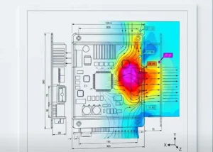
Printed circuit boards (PCBs) serve as conductive patterns that connect electronic components; They provide mechanical support for these components while also establishing electrical connections according to predefined circuit layouts and acting as insulators.
The modern electronics industry relies on PCBs, which serve as foundational components for communications, computing, automotive, industrial control, medical device, defense and aerospace applications.
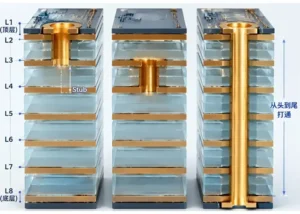
Via holes, as key structures connecting conductive paths between different layers of multilayer PCBs, are crucial to circuit reliability and signal integrity.
However, the PCB manufacturing process is complex, involves numerous steps, and has stringent technical requirements.
If not properly controlled, it is highly prone to via defects such as plating voids, via wall fractures, inner layer delamination, and rough via walls.
In particular, in recent years, with the trend toward miniaturization of packaging and higher-density interconnects, the fabrication of small-diameter (≤0.15 mm) and high aspect ratio (≥10:1) through-holes.
This creates several electroplating challenges. The plating solution may not fully fill the hole cavity, and trapped air can prevent proper venting. Earlier drilling problems can also cause hole misalignment and wall damage when the drill bit breaks.
Ultimately, these issues result in increased product resistance, signal attenuation, or even open-circuit failures.
Although industry standards (such as IPC-A-600[2]) have established clear requirements for through-hole quality, interconnection defects caused by fluctuations in process parameters, insufficient material compatibility, or improper process control remain common in actual production.
Based on typical cases of through-hole interconnect failures, this paper conducts an in-depth analysis of the failure causes and mechanisms through microscopic characterization, thermal performance testing, and process quality verification.
It also proposes targeted process optimization strategies to mitigate quality and reliability issues caused by through-hole defects.
Samples and Testing
-
Sample Information
The failed sample was an automotive printed circuit board assembly (PCBA).
During whole-unit screening tests conducted at room temperature, the sample exhibited open-circuit failures in the green solder mask via holes 1 to 2 hours into the test, with a failure rate of 0.5%.
The PCBA was manufactured using a soldering process that involved double-sided reflow soldering followed by wave soldering.
-
Sample Testing
We conduct a series of tests and analyses to identify the failure modes of defective samples.
1. Metallographic Section Analysis
In accordance with the requirements of IPC TM-650 2.1.1F, testing was conducted according to the following steps.
a) We fully encapsulate failed plug samples with epoxy cold-embedding resin to avoid deformation and damage during specimen preparation and guarantee accurate cross-sectional observation results.
b) Using an ASIDA-YM22 metallographic grinding and polishing machine, along with sandpaper and polishing consumables, prepare the plug-hole cross-section following the sequence: coarse grinding → fine grinding → coarse polishing → fine polishing → etching.
This ensures the cross-section is clean, flat, and free of scratches, clearly revealing its true morphology.
c) First, observe the overall morphology of the cross-section and locate abnormal areas using an Olympus BX53M metallographic microscope.
Then, use a scanning electron microscope (SEM) to magnify and examine the area, analyzing microscopic features such as the fracture morphology and grain.
2. Thermal Shock Validation
We perform the test per the IPC TM-650 2.6.7.2B standard. This test selects 100 PCB specimens from a single batch.
All samples are placed in a TS120SW thermal shock test chamber, with test parameters configured as follows: the low-temperature stage is set to -25 °C and the high-temperature stage to 75 °C.
The dwell time at each temperature extreme was 30 min; the entire test consisted of 10 temperature cycles.
We measure the resistance of all samples after the test to screen out specimens with abnormal resistance.
We then prepare microsections from defective samples and observe their microstructure via a metallographic microscope to analyze internal structural damage induced by thermal shock.
3. Thermal Performance Testing
We carry out the test following the IPC-TM-650 2.4.24C standard.
All test samples are classified into two groups: failed specimens and qualified bare boards manufactured in the same batch period.
During the sample preparation stage, both types of samples underwent surface pretreatment to remove the green solder mask coating and the top layer of copper foil, thereby eliminating the interference of surface impurities on the test results.
Subsequently, a TMA 402F3 thermomechanical analyzer was used to conduct Z-axis coefficient of thermal expansion (CTE) testing.
To guarantee test accuracy, we bake the samples at 105 °C for 2 hours before testing to completely eliminate internally adsorbed moisture.
During the test, the temperature scanning rate was set to 10 °C/min to ensure uniform temperature changes and stable data acquisition.
Test Results
-
Analysis of the Axial Cross-Section of the Plug Hole
We prepare microscopic sections to observe the authentic microstructure of the plug hole axial cross-section, which provides direct evidence for visual evaluation of potential cross-sectional defects.
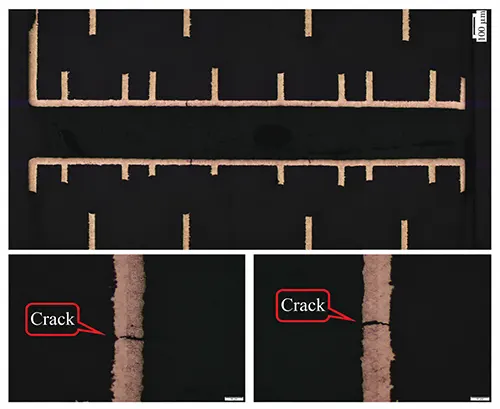
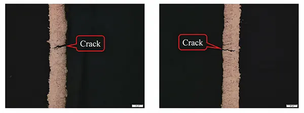
The metallographic microscope image of the cross-section of a failed plug hole is shown in Figure 1. The results indicate:
a) Fractures symmetrically distributed on the central copper lining of the plug hole wall are clearly observed.
b) Upon magnified examination of the fracture area, the crack patterns on both sides of the fracture surface matched well;
c) We observe no obvious tensile deformation on the copper lining at fracture locations.
The copper lining of failed plug holes presents a relatively uniform thickness distribution, with an average thickness of 24 μm.
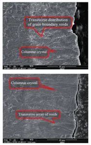
To further analyze its microstructural characteristics, SEM was used to characterize the coating on the axial cross-section of the plugged hole at high magnification.
The results are shown in Figure 2, which reveal that:
a) Numerous columnar crystals distribute at the interface between the copper coating and the substrate.
b) Void defects exist along the grain boundaries of columnar crystals and present a transverse arrangement.
-
Temperature Shock Validation
Temperature fluctuations cause the PCB substrate to undergo periodic contraction and expansion, and the resulting axial stress continuously exerts a tensile force on the through-holes.
When this stress exceeds the tensile strength threshold of the through-hole, it can lead to cracking or even fracture of the through-hole;
Once a through-hole fails, it typically exhibits electrical behavior characterized by increased conduction resistance or a complete open circuit.
This study explores the influence of alternating hot and cold environments on PCB through-hole reliability.
We conduct thermal shock tests to monitor resistance variations in PCB through-holes and perform metallographic sectioning to observe their cross-sectional morphology.
The combination of two methods reveals the failure mechanisms of through-holes under temperature cycling.
We select specimens from the same batch as the failed samples and measure their conductance before and after thermal shock testing.
The test results showed that, out of 100 test samples, 8 exhibited failure characterized by a significant increase in resistance or an open circuit; the conductance test results are shown in Table 1.
A representative cross-section of a failed via after the thermal shock test is shown in Figure 3.
| Failed Sample | Conductive Resistance Before Test (Ω) | Conductive Resistance After Test (Ω) | Change Rate |
|---|---|---|---|
| #1 | 0.001970 | 1.011364 | 51,238.27% |
| #2 | 0.001933 | 0.105937 | 5,380.44% |
| #3 | 0.001852 | 1.024850 | 55,237.47% |
| #4 | 0.001987 | 1.972840 | 99,187.37% |
| #5 | 0.001996 | 2.103934 | 105,307.52% |
| #6 | 0.001899 | 1.097832 | 57,711.06% |
| #7 | 0.001876 | 0.906458 | 48,218.66% |
| #8 | 0.001942 | Open Circuit | / |
Table 1. Conductive Resistance Test Results of Failed Samples Before and After Thermal Shock
-
Thermal Performance Testing
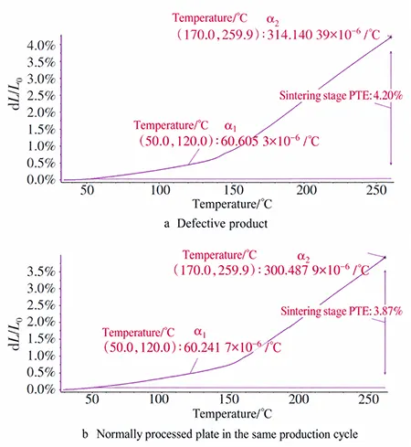
We perform Z-CTE tests on failed samples and contemporarily produced normal uncoated panels to evaluate the Z-axis thermal expansion and contraction properties of PCB panels.
The thermal mechanical analysis (TMA) curves obtained from the tests are shown in Figure 4.
Parameters such as the CTE of the substrate below the glass transition temperature (Tg) (i.e., α1-CTE), the CTE above Tg (i.e., α2-CTE), and the percentage of thermal expansion along the Z-axis (PTE) are shown in Table 2.
| Sample | α1-CTE / °C⁻¹ | α2-CTE / °C⁻¹ | PTE |
|---|---|---|---|
| Failed Sample | 6.06 × 10⁻⁵ | 3.141 × 10⁻⁴ | 4.20% |
| Plate from the Same Production Cycle | 6.02 × 10⁻⁵ | 3.005 × 10⁻⁴ | 3.87% |
Table 2. Z-CTE Test Results
Discussion and Analysis
-
Failure Mechanism Analysis
Based on the above test results, it is evident that the failed plug holes exhibit distinct microscopic defects and failure pathways:
1. Microscopic Characteristics of Failed Plug Holes
The copper in the central portion of the plug hole walls exhibits a symmetrical fracture pattern;
We observe abundant columnar crystals at the interface between copper plating and the substrate, with transverse voids distributed along the grain boundaries of these crystals.
The columnar crystal defects primarily stem from the anisotropy of nucleation during the electroplating process:
If issues such as uneven plating bath flow rates or variations in current density distribution occur, the plating layer will preferentially grow perpendicular to the substrate, forming an oriented arrangement of columnar crystals.
The formation of transverse grain boundary voids is directly related to defects in the post-electroplating heat treatment process:
If the heat treatment temperature is too low or the holding time is insufficient, residual hydrogen within the plating layer cannot fully escape and will accumulate at the grain boundaries of the columnar crystals, forming voids;
Furthermore, the adsorption of impurity ions in the plating solution weakens grain boundary bonding strength, further exacerbating the nucleation and propagation of voids.
2. Mechanism of Crack Initiation and Propagation Under Axial Stress
The oriented arrangement of columnar grains inherently reduces the isotropy of the perforated copper, making the grain boundaries areas of mechanical weakness.
Voids at the transverse grain boundaries further weaken the grain boundary bonding strength, significantly reducing the tensile strength and ductility of the perforated copper and markedly increasing its brittleness.
When axial stress is applied to the plated copper, stress preferentially concentrates at grain boundary voids, whose stress concentration factor rises with increasing void size, thus inducing intergranular fracture of columnar grains.
The grain boundary bonding strength at the voids is insufficient to resist the stress, causing the grains to separate and ultimately leading to the fracture of the perforated copper.
Fracture damages the electrical pathways of plated copper, resulting in increased resistance and even open-circuit failure.
3. Substrate Thermal Expansion Effect and Standard Correlation Analysis
Further evaluate the impact of thermal expansion of the substrate on failure in conjunction with industry standards:
According to IPC-4101E, substrates suitable for lead-free soldering processes must meet the following Z-CTE requirements: α1-CTE (below Tg) must not exceed 6.0×10⁻⁵/°C, and α2-CTE (above Tg) must not exceed 3.00×10⁻⁴/°C, and the Z-PTE must not exceed 4.0%.
A comparison of test data shows that the Z-CTE values for both the failed samples and the normal samples from the same production batch were slightly higher than the specified limits.
However, for through-holes without microscopic defects and with an average copper wall thickness of 20 μm or more, slight exceedances of the thermal expansion limits in the substrate typically do not cause copper wall fractures;
For failed products that already exhibit columnar grain boundary voids, the vertical stress generated by the thermal expansion and contraction of the sheet acts as a “stress trigger,” exacerbating the risk of through-hole copper fracture and serving as a key contributing factor to their failure.
To conclude, the core failure mechanism chain accounting for plug-hole defects in this batch of PCBs is outlined as follows:
Improper control of the electroplated copper process → formation of columnar grains and transverse grain boundary voids in the copper plating → reduced axial tensile strength and ductility of the through-holes → thermal expansion and contraction of the sheet, combined with axial stresses during environmental or operational phases→ fracture of the copper plating in the plugging holes → ultimately resulting in an open-circuit failure.
-
Analysis of Key Process Risks and Recommendations for Improvement
Based on the principles of the electroplating process, the potential factors contributing to the formation of columnar crystals and grain boundary voids in the copper plating on holes, along with corresponding improvement methods, are as follows.
1. Analysis of Key Process Factors and Recommendations for Improvement
a) Abnormalities in the Electroplating Bath System
The primary methods for addressing abnormalities in the plating bath system are as follows:
Regularly test the composition of the plating bath using titration or online monitoring instruments, and replenish main salts and additives according to standards to ensure concentrations remain within the process window;
Installing a plating solution filtration system (such as activated carbon filtration or precision filter cartridge filtration) to regularly remove metal impurities and organic contaminants, and perform a comprehensive purification of the plating solution after each production batch.
b) Improper Control of Process Parameters
Improper control of process parameters includes unreasonable settings for electroplating current density and voltage, as well as inaccurate regulation of the plating bath temperature.
We adopt targeted optimization methods to rectify the unreasonable control of process parameters.
We optimize the current density curve based on the pore size and substrate thickness, and implement a stepped current strategy for electroplating.
Specifically, low current is applied for seed layer deposition, and medium current is used for copper layer thickening.
This method prevents abnormal crystallization induced by localized current spikes.
And installing a high-precision temperature control system (such as a proportional-integral-derivative [PID] temperature controller) to maintain bath temperature fluctuations within ±1 °C, thereby ensuring a stable crystallization rate.
c) Defects in Pretreatment and Process Control
Defects in pretreatment and process control include incomplete pretreatment of the substrate, resulting in residual oil and oxide layers on the surface;
Insufficient agitation of the plating bath, leading to uneven ion concentrations on the cathode surface.
Methods to address these defects in pretreatment and process control include:
We optimize the pretreatment process through two key improvements.
First, ultrasonic degreasing is performed at a power of 500–800 W. Second, a micro-etching treatment with a concentration of 30–50 g/L is newly added.
A water film test is used to verify substrate surface cleanliness, where a continuous water film duration of no less than 15 s is regarded as the qualification standard.
Upgrade the plating bath agitation system by combining air agitation with mechanical agitation to ensure uniform agitation rates (30–50 r/min), and regularly inspect the wear on the agitation blades, replacing them promptly when necessary.
2. Analysis of Other Common Failure Factors and Recommendations for Improvement
In addition to the hole-plugging fracture failures caused by columnar crystals and grain boundary voids described earlier, common causes of hole-plugging failure include the following categories.
a) Glass Fiber Fracture
During drilling, excessive milling cutter wear, mismatched rotational speed, or inappropriate feed rate can all lead to tearing of the glass fibers on the hole wall.
The bond strength between the copper plating and the substrate near the damaged glass fibers is reduced, which in turn affects the tensile strength of the copper in that area of the via.
Methods to mitigate glass fiber breakage include:
1) Replacing the milling cutter on time based on its wear condition;
2) Selecting spindle speeds and feed rates appropriate for the product based on machining conditions;
3) Using suitable cooling and lubrication methods during machining.
b) Ineffective Removal of Resin Residue
If drilling residue is not thoroughly removed, the adhesion between the copper plating and the substrate in areas containing resin residue is poor during the copper plating process.
Under thermal stress, this can easily lead to delamination of the hole walls.
Additionally, residual resin may affect the quality of subsequent copper plating, causing issues such as uneven plating thickness.
The primary methods for improving the effectiveness of resin residue removal include:
1) Strictly controlling key parameters such as the concentration, temperature, and duration of the resin remover;
2) Adopting a process that combines multiple resin removal methods, such as using plasma resin removal in conjunction with chemical resin removal;
3) Adding auxiliary cleaning steps, such as ultrasonic cleaning.
c) The Giavanni Effect
During the PCB manufacturing process, when two electrically conductive metals (such as copper and gold) coexist on the board surface, a significant potential difference arises between them in an acidic environment, forming a galvanic cell.
The metal with the lower potential (copper acts as the anode) loses electrons more rapidly, resulting in metal etching.
If the etched metal is the copper plating on a through-hole, the copper plating in that area will become thinner, creating a risk of fracture in the through-hole under stress.
The main methods for mitigating the Giavanni effect are:
1) Selecting an appropriate chemical solution system during the manufacturing process to keep the Giavanni effect within a reasonable range;
2) Increasing the thickness of the gold layer in the chemical nickel-gold plating process.
Conclusion
Through a systematic analysis of key factors—including the microstructure of the plugged via cross-sections in failed products and the thermal properties of the substrate—this paper reaches the following core conclusions:
Owing to oversights in the control of the copper plating process by PCB manufacturers, microscopic defects—such as columnar crystals and transverse intergranular voids—form within the copper plating of the via holes.
Multiple stresses jointly act on the substrate during the service process.
These stresses include soldering thermal expansion stresses, ambient temperature variation stresses, and axial stresses in actual operation.
The combined force triggers intergranular separation between copper grains.
This defect further causes typical electrical failures of via holes. Common failures include increased circuit resistance and complete open circuits.
Fracture of the copper plating in PCB vias directly threatens the quality and reliability of electronic products.
Based on actual failure cases, this paper provides an in-depth analysis of the underlying failure mechanisms of via copper fractures and proposes targeted process improvement measures.
In practical production scenarios, electronics manufacturers need to analyze factors causing common production defects.
They must fully consider the contribution of various defect-inducing factors.
Refined and stricter production control measures should be implemented.
These measures cover process optimization, production equipment maintenance and upgrading, and end-to-end quality monitoring.
They also include precise production environment control and high-quality raw material selection.
Such targeted controls eliminate and reduce similar quality problems from the source.