As electronic product designs become increasingly sophisticated and intelligent, the components to be inspected on PCBs are arranged in ever-denser patterns, and chip pin sizes are becoming smaller and smaller.
Consequently, the ability to detect placement errors and soldering defects is continuously improving in line with the manufacturing industry’s pursuit of higher product quality.
Evolution of PCB Inspection Technology and Advantages of 3D-AOI
Inspection methods for PCBs have evolved from manual visual inspection (MVI) and automated visual inspection (AVI) to automated optical inspection (AOI).
Within the AOI field, there has been a clear trend toward technological iteration, shifting from 2D planar inspection to 3D stereoscopic inspection.
The introduction of 3D-AOI imaging technology, which provides highly precise information, not only enhances the accuracy of 2D inspection but also ensures that complex defects—such as lifted pins, raised components, and solder wicking—can no longer go undetected.
Limitations of Conventional 3D-AOI Visual Inspection
Traditional visual inspection processes involve many variables—such as lighting, color variations, curved surfaces, and differences in field of view—that are difficult for machines to recognize.
This requires process operators to possess extensive prior knowledge of quality control and experience in defect detection.
The development process is cumbersome, the systems have poor environmental adaptability, and they tend to be overly strict, resulting in high false rejection and false positive rates.
This directly leads to traditional 3D-AOI inspection equipment being difficult to program, prone to false positives, and inefficient.
AI-Driven 3D-AOI for Intelligent PCBA Full-process Quality Control
With the widespread adoption of artificial intelligence technology, the 3C quality inspection sector has undergone revolutionary changes, and AI has gradually become a key enabler in the field of intelligent quality inspection.
Advancing and accelerating the development of AI infrastructure is a core task of the “New Infrastructure” initiative and serves as a vital foundation for supporting technological self-reliance and the development of the digital economy.
AI-enabled 3D-AOI inspection equipment utilizes deep learning algorithms at its core to create unified models for various defect types, thereby building a large-scale knowledge base of process defects.
Through graphical user interfaces and minimalist configuration, it enables rapid, intelligent programming and operation.
With high environmental tolerance and inspection accuracy and efficiency that surpass manual inspection, it performs 3D optical automatic inspection tasks more intuitively and scientifically, comprehensively strengthening quality control throughout the entire PCBA production process.
Overview of 3D AOI Technology
3D AOI equipment calculates continuous phase by projecting multiple sine gratings with different phases and uses phase-modulated contour measurement technology to perform 3D topography measurements on precision components.
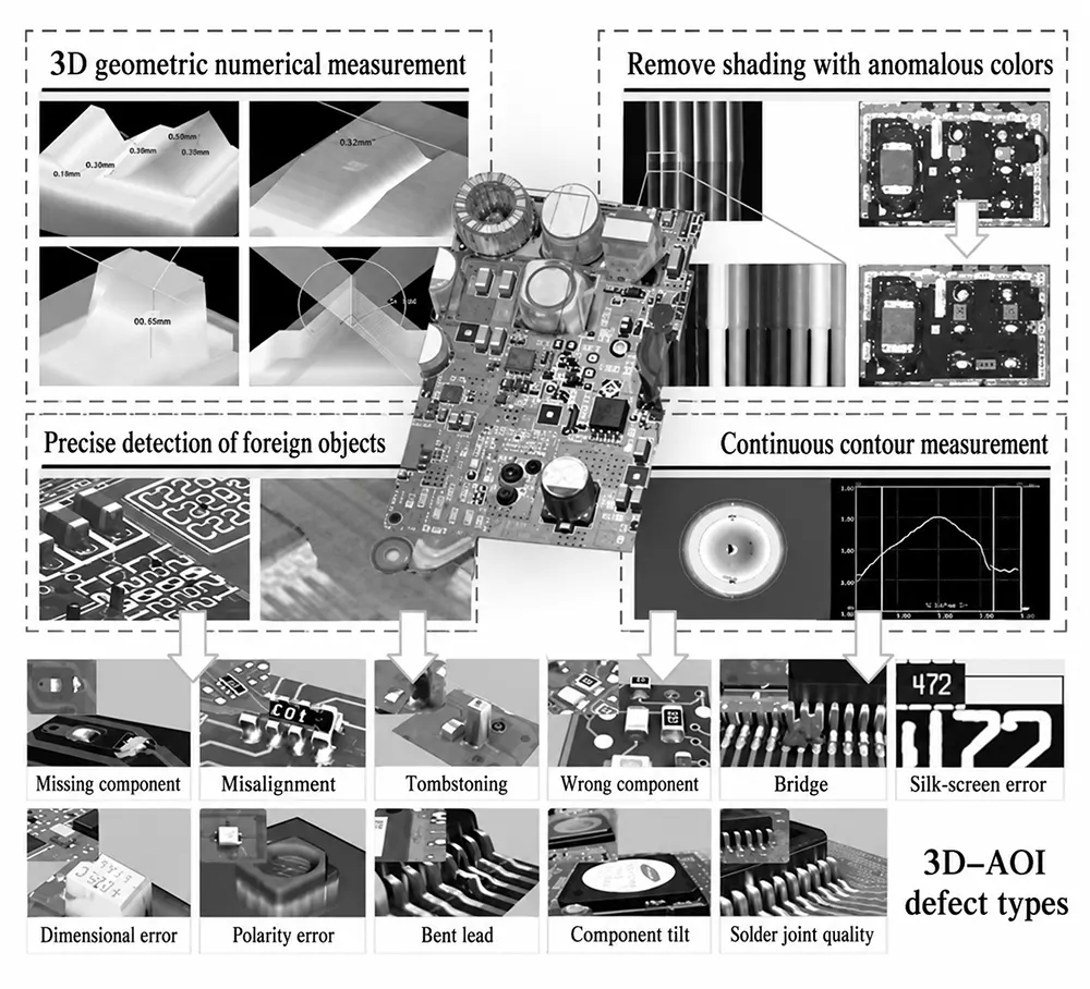
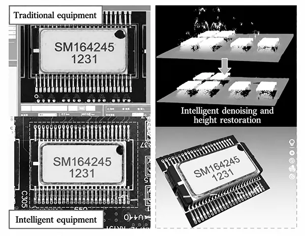
As shown in Figure 1, advanced 3D-AOI imaging technology can eliminate halo shadows while preserving excellent color reproduction, resulting in high-resolution color images.
Through measurements based on 3D geometric digitization, it can comprehensively inspect the contour shapes of targets, capture subtle deformations, and accurately identify foreign objects not part of the assembly based on 3D data.
By incorporating height information into two-dimensional images, 3D AOI equipment can accurately detect defects in surface-mount components and solder joints.
While precisely identifying missing components, misalignment, tombstoning, incorrect components, dimensional issues, polarity errors, and bridging, it also detects complex defects such as component lead warping, lifting, tilting, and solder ball defects.
Intelligent 3D-AOI equipment, enhanced with AI technology, learns from a vast number of positive and negative samples to autonomously identify deep-level features, master the standard geometric characteristics of components, and understand the variations and severity of these characteristics under various conditions.
It intelligently calculates algorithm parameters and judgment rules to make effective decisions, significantly reducing the programming workload.
Comparison of the Advancements in Intelligent 3D-AOI Technology
Intelligent 3D-AOI inspection equipment typically consists of three components: a high-precision motion platform, an advanced image acquisition system, and a user-friendly intelligent programming interface.
The user-friendly programming is easy to learn, the intelligent algorithms minimize false positives, and the equipment is stable and highly efficient.
High-Precision Motion Mechanism
The high-precision motion mechanism enables automatic module loading and rapid optical scanning.
In traditional equipment, the Z-axis range is fixed, making it impossible to clearly capture images of components taller than 5 mm;
Track vibrations and operating speeds can also cause vignetting and substrate unevenness.
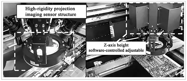
In contrast, the smart device features a wide, adjustable range along all three axes (X, Y, and Z), allowing the Z-axis height to be adjusted to match the optimal height for different component heights.
The highly rigid projection sensor structure significantly reduces product vibration during high-speed operation and provides micron-level motion accuracy, as shown in Figure 2.
Additionally, the system is equipped with a substrate height adaptive correction algorithm that captures the clearest possible images, facilitating defect detection and fully meeting the clear inspection requirements for both standard carriers and components under 40 mm in height.
Advanced Image Acquisition
The advanced image acquisition module generates high-definition images in real time and enables rapid 3D data analysis.
In traditional equipment, the colors in the imaging interface generally have an orange-red cast, making it difficult to distinguish details during the re-inspection process;
Furthermore, traditional algorithms require layer-by-layer color extraction from the substrate and components before programming, which is time-consuming and results in low accuracy.
In contrast, the smart device uses projection imaging from four directions. It applies a reflection compensation algorithm to minimize shadows.
It also uses phase consistency among corresponding points across multiple views. This approach intelligently removes outlier noise from depth maps.
The colors displayed on the imaging interface faithfully reproduce the product’s original appearance, with defects appearing in stark contrast, significantly improving the efficiency of inspectors’ re-evaluation;
At the same time, it easily locates circuit boards at any angle or position.
After capturing an image, it automatically distinguishes between the substrate color, pad color, and silkscreen color.
Once programming begins, 3D modeling of components can be performed immediately, allowing for direct programming and analysis using defect detection algorithms;
This solution offers greater versatility and a broader inspection range for products with substrate backgrounds that match the color of the components.
Minimalist Smart Programming
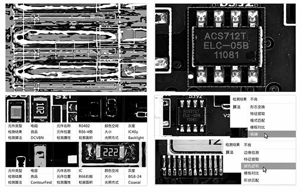
The Minimalist Smart Programming section enables rapid batch programming and intelligent defect detection.
Intelligent 3D-AOI equipment eliminates the numerous tedious operations involved in traditional programming—such as repeatedly drawing frames, extracting colors layer by layer, configuring lighting, adjusting vectors, and manually separating characters one by one.
As shown in Figure 4, the software intelligently matches the relationships between lighting, vectors, algorithms, and defect types, reducing the prior knowledge required by inspectors for programming and significantly lowering the learning curve for operating the equipment.
1. Comparison of Programming Modes Between Traditional AOI and Intelligent 3D-AOI
Traditional equipment identifies target components one by one during the programming process based on grid-based positioning files.
However, the appearance of different types of components varies depending on the field of view, lighting conditions, and surface curvature.
This requires algorithms to capture component features from multiple dimensions and manually delineate detection boxes for target areas one by one—a cumbersome process that results in inflexible algorithm models that are difficult to optimize.
In contrast, smart devices can perform pixel-level classification based on the semantic information in images, automatically selecting common components.
They offer strong detection capabilities and generalizability, and can intelligently correct misclassifications caused by variations in component shapes.
2. Deep Learning-based Automatic Feature Extraction for Simplified Programming
AI-powered algorithms use deep learning to reduce the need for manual feature extraction or rule definition, automatically learning features from a massive dataset of raw positive and negative samples to accelerate programming.
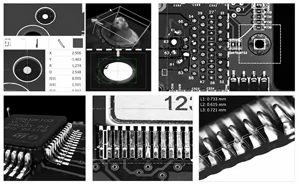
Specifically, for the programming of solder joints and mark points—as shown in Figure 5—intelligent AOI algorithms can automatically select solder joints and chips with a single click and intelligently configure generic parameters.
3. Batch Parameter Copying and Precise Defect Localization via Array Broadcasting Algorithm
After completing the parameter modeling for the first pin, the intelligent AOI system employs a fast, batch-processing array broadcasting algorithm.
This algorithm features automatic image alignment during the parameter copying process, allowing feature parameters to be copied in a single step without the need to manually add or calculate the number of pins or their spacing.
Ultimately, during the defect detection phase, the intelligent system can directly locate the specific pin where the defect occurs, significantly improving the accuracy of re-inspection.
Autonomous Learning and Defect Retrospection
Intelligent AOI equipment provides an edge-side AI training platform that enables rapid, small-sample training for new components and defect types at the tail end of the data distribution.
This allows the equipment to continuously refine its recognition of different component forms, effectively reducing the false positive rate and enabling rapid iteration and continuous upgrades to inspection capabilities.
Through the device-based SPC analysis tool, process data for products can be recorded and analyzed throughout the entire production cycle.
This enables intelligent early warnings and automatic shutdowns when consecutive defects occur at the same location on the same product, alerting operators to inspect the product.
At the same time, the system can automatically generate detailed inspection reports that visually present timestamps, defect locations, specific defect information, and raw images through a combination of text and graphics.
Additionally, it supports remote viewing and data traceability, significantly reducing the workload associated with manual data compilation.
By deeply analyzing defect data characteristics during the inspection process, the system provides critical data support for improving front-end production processes and optimizing inspection models.
It continuously enhances understanding and accumulation of knowledge regarding AOI scenarios, tracing processes, and design issues through defect analysis.
Deploying intelligent AOI equipment before and after the PCBA reflow oven enables the detection of defects such as missing components, reversed components, lifted pins, and excessive height.
Scope of Application for Intelligent AOI Technology
Intelligent AOI equipment uses deep learning to accurately extract a vast number of defect features and rapidly complete model transfer through AI technology.
In addition to defect detection capabilities for PCBs, the autonomous learning, high generalizability, and low false positive rate of intelligent AOI equipment enable this technology to cover various typical process defects throughout the entire product lifecycle during production quality inspection.
Currently, printed circuit board production is becoming increasingly miniaturized and precision-oriented, with lines growing finer, via diameters shrinking, and pattern spacing becoming denser.
Deploying intelligent 2D-AOI equipment optimized with deep learning algorithms during the board etching stage enables the detection of subtle defects such as open circuits, short circuits, notches, etching defects, thick line violations, and via blockage failures.
After solder paste printing on the PCB, 3D-AOI equipment is deployed to perform SPI inspection, enabling the detection of defects such as insufficient solder, excess solder, solder peaks, and poor solder paste patterns.
During the conformal coating stage, specialized UV lighting and intelligent 2D-AOI equipment are deployed to automatically identify coating areas and detect defects such as over-coating, under-coating, bubbles, splatter, and foreign objects.
As application scenarios and scope continue to expand, AI-enabled AOI inspection models can continuously learn about new components and solder joints, resulting in constantly upgraded testing capabilities and rapid iteration.
Conclusion
Intelligent 3D-AOI technology can accurately extract defect features based on deep learning and autonomously identify inspection areas through AI models, thereby reducing the false positive rate of traditional AOI equipment and improving first-pass yield.
Researchers widely apply intelligent algorithms for industrial inspection. They use big data analytics to continuously optimize inspection models.
This cuts programming steps and parameter adjustments for equipment.
It lowers the learning threshold for process operators. It reduces manual re-inspection work. This directly decreases product manufacturing costs.
This technology has a wide range of applications and use cases, significantly improving inspection efficiency on the production floor, optimizing manufacturing costs, and reducing reliance on manual labor.
While reducing labor costs associated with inspection and re-evaluation, it greatly increases inspection speed, with overall programming efficiency improving by 60% and inspection speed increasing 5 to 10 times compared to manual inspection.
This achieves value creation through quality improvement, cost reduction, and efficiency gains.