Manufacturers produce conventional flexible printed circuits mainly by subtractive processes.
These workflows contain complicated procedures. They include seven core processes and over 70 total steps.
The processes also create massive material waste and serious heavy metal pollution.
Traditional processes and 3D printing suffer from low precision (100–150 μm), high curing temperatures (350 °C+), and insufficient electrical conductivity.
This project focuses on additive manufacturing technology for flexible circuit boards, aiming to address industry challenges such as material waste, environmental pollution, process complexity, poor precision, and high curing temperatures.
It has successfully developed China’s first high-flow piezoelectric additive manufacturing technology for flexible circuits.
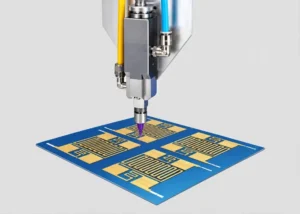
Researchers develop an automatically controlled intelligent printing platform for flexible printed circuits in this project (see Figure 1).
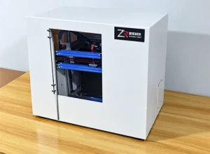
The platform integrates three core technologies. This greatly optimizes the production process of flexible circuits.
The platform carries piezoelectric microfluidic printheads. It identifies uploaded circuit drawings.
It realizes uniform and accurate jet printing. This manufactures small-batch and customized flexible circuit patterns.
The production process is environmentally friendly, pollution-free, and waste-free;
Researchers develop low-melting-point alloy ink for additive manufacturing.
This innovative alloy material scheme breaks new ground. It raises production efficiency and product quality for FPCs.
It also boosts circuit conductivity by over 40%.
This technology is primarily applied in emerging industries such as artificial intelligence, medical devices, and new energy vehicles;
We have developed supporting operating systems and automated inspection systems to ensure the most comprehensive reading of circuit files.
With over 50 inspection items throughout the entire process, these systems guarantee consistency between the printed circuit and the design.
They can test key metrics such as peel strength, flexural strength, tensile strength, elongation, and coefficient of thermal expansion, enabling high-precision control of the circuit.
Technical Principles and Functions
Piezoelectric Microfluidic Technology
Piezoelectric microfluidic technology is a novel technology developed by the project team.
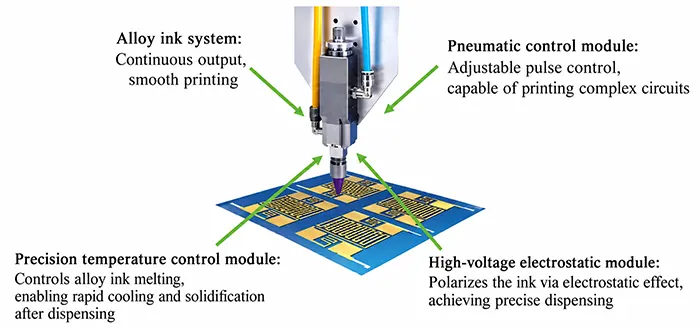
It relies on the piezoelectric effect to achieve precise ink control, as shown in Figure 2.
A drive voltage waveform is applied via a function generator, causing the quartz crystal inside the piezoelectric chamber to contract or expand, thereby generating an electrostatic force that ejects a micro-volume of ink.
This is combined with a proprietary low-melting-point alloy ink that cures and sets at low temperatures.
This technology ingeniously overcomes the limitation of the quartz crystal’s low positive dielectric constant, resolving issues such as unstable ink ejection and inaccurate dosing in traditional direct-writing methods.
It improves printing parameters by over 40% and offers advantages such as a high natural frequency and excellent dynamic response, enabling highly efficient and precise wiring.
Low-Melting-Point Graphene Alloy Ink
In collaboration with the School of Chemical Engineering and Materials Science, our team conducted tens of thousands of experiments to develop a low-melting-point graphene alloy ink.
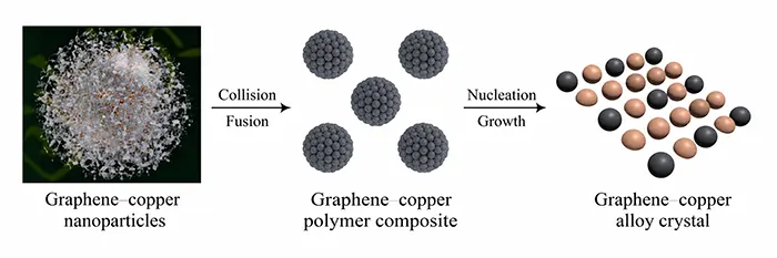
Researchers adopt the graphene-alloy microsphere process shown in Figure 3.
They select graphene nanosheets as the reinforcing phase and high-purity copper powder as the matrix.
They adjust key parameters including ball-to-material ratio and rotational speed. This completes powder preparation via ball milling.
This ink supports particle size control from 1 to 10 μm. It has high sphericity, low melting point, and high solid content.
These features greatly improve electrical conductivity. The ink satisfies low-temperature curing requirements.
Inkjet Printing Multi-Dimensional Control System
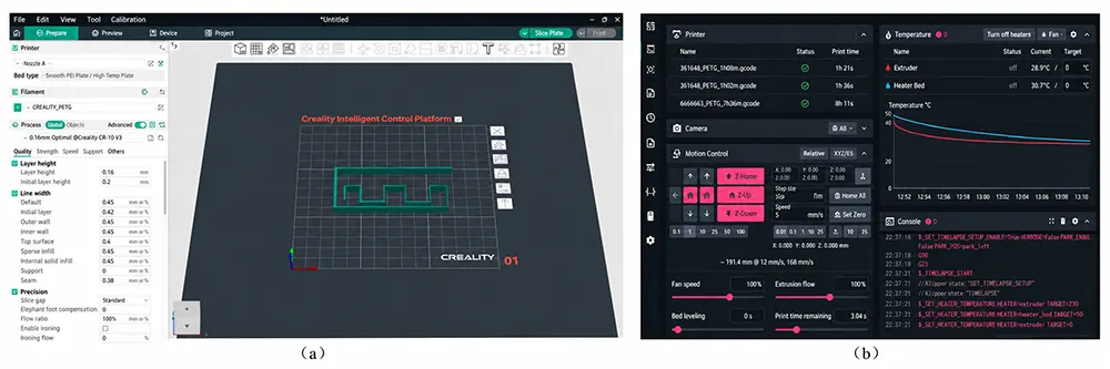
To enhance the high fidelity of circuit slice reading by the control system during the printing process and the precision of three-axis control, the team jointly developed a full-process monitoring system, as shown in Figure 4.
The system includes control software and inspection software, and employs an AI vision model to train an intelligent inspection system.
By integrating the DeepSeek large-scale model, it comprehensively safeguards circuit production and effectively improves circuit printing quality.
Relying on a material property database, the control software dynamically adjusts process parameters.
It adopts finite element analysis to achieve adaptive structural adjustment and optimizes multi-axis coordinated control via the D-H parameter method and genetic algorithms.
The system achieves a printing accuracy of ±5 μm, with a minimum line width of 20 μm.
By relying on closed-loop visual feedback to correct deviations in real time, the yield rate has increased by 20% to 30%.
The inspection software covers more than 50 key parameters, comprehensively ensuring the quality and consistency of circuit printing.
Innovative Features and Market Prospects of the Product
This project introduces China’s first-of-its-kind additive manufacturing equipment for flexible circuits.
Engineers take the piezoelectric microfluidic printhead as the core component.
They use low-melting-point alloy ink as functional material. A multi-axis control system supports the whole system.
They build an integrated additive manufacturing system.
This system features “precision drive — material adaptation — spatial shaping.”
This system fabricates high-precision, complex three-dimensional metallic microstructures.
The printed FPCs surpass competing industrial products.
They show better performance in processing accuracy, uniformity, surface smoothness, and electrical conductivity.
The project’s innovatively developed low-melting-point graphene alloy ink enhances the product’s electrical conductivity by more than 40 percent.
Coupled with a multi-dimensional inkjet printing control system, it guarantees a circuit line precision of 50 μm, ensuring that the printed circuits closely match the design specifications.
Through advanced additive manufacturing processes, the project significantly improves efficiency and reduces costs while maintaining product quality and performance.
The products have received ILAC-MAR international accreditation and are expected to bring revolutionary changes to the electronics manufacturing industry in China and around the world.