The performance characteristics of printed circuit boards (PCBs) originate from their design, while transforming that design into a finished PCB relies on the manufacturing process.
Successful manufacturing hinges on the critical factor of manufacturability.
For decades, manufacturability reviews of PCB designs have been an essential step.
As product types and technical requirements evolve, manufacturability demands continue to change.
This section introduces some fundamental, conventional knowledge.
Design for Manufacturability (DFM)
Design for Manufacturability (DFM) refers to a practice in PCB design.
In this approach, engineers not only meet functional requirements but also thoroughly consider the feasibility of manufacturing to ensure compliance with manufacturability conditions.
The primary goal of PCB design is to achieve electrical and mechanical functional requirements.
However, a comprehensive approach must also incorporate DFM, Design for Assembly (DFA), Design for Testability (DFT), and Design for Reliability (DFR).
Collectively, these constitute Design for Excellence (DFX).
While each focus is distinct, their content interrelates. Designers achieve DFX in PCB design by addressing four aspects: functionality, DFR, manufacturability, and cost-effectiveness.
This means the PCB delivers the desired functionality, operates reliably, supports efficient manufacturing, and can be produced at a relatively low cost.
The essence of DFM primarily lies in manufacturability and cost-effectiveness, specifically production capability and manufacturing cost.
Its purpose is to ensure that manufacturers can produce the designed PCB smoothly and economically.
DFM must permeate the entire PCB design process. Considerations must extend from PCB structural dimensioning and substrate selection to circuit layout and surface finishes:
Is it technically feasible? Is the economic cost justified? In other words, how manufacturable is it?
While ensuring the PCB delivers the required functionality, designers must select appropriate PCB types, structural dimensions, circuit patterns, and substrate materials.
Basic Principles of DFM
PCB design has evolved from manual, human-dependent methods to continuous advancements in Electronic Design Automation (EDA) and Computer-Aided Design (CAD).
Today, PCB design has entered the era of Artificial Intelligence (AI).
Facing increasingly complex design demands, AI enhances both quality and efficiency in PCB design, achieving a new leap forward.
However, the fundamental principles for ensuring Design for Manufacturing (DFM) remain unchanged.
-
Designers Should Possess Fundamental Knowledge of PCB Manufacturing
Designers should understand basic PCB manufacturing principles.
They should be familiar with PCB design and finished product standards, comprehend manufacturer capabilities, and know how to translate designs into tangible products.
If PCB design files are generated by AI, then this foundational knowledge must also be “instilled” into the AI to enable it to design optimal PCBs.
The essential knowledge required for training is as follows.
1.Functions and Types of PCBs
PCBs come in a wide variety of types. Designers should select the appropriate type based on specific application requirements.
2.PCB Manufacturing Processes
PCB manufacturing processes primarily include subtractive, semi-additive, and additive methods.
The subtractive process represents the traditional method for copper-clad laminates. In this process, manufacturers selectively etch copper foil to form circuits.
The semi-additive process involves depositing a copper layer onto an insulating substrate, followed by selective etching of the copper layer to form circuits.
The additive process directly deposits conductive material onto the insulating substrate to form circuits.
Manufacturers select different process routes based on the specific design requirements of the PCB.
3.Product Standards
Product standards represent universally recognized quality requirements within the industry.
Typically, finished PCB standards encompass specifications for appearance, dimensions, electrical performance, mechanical properties, and environmental factors.
Classification standards are based on PCB types.
Additionally, these standards include PCB design specifications and substrate specifications, all of which constitute fundamental prerequisites for meeting finished product specifications.
PCB standards vary by geographic scope: international (IEC), national (China’s GB and GJB, U.S. ANSI and MIL), industry (China’s SJ), group (China’s CPCA, U.S. IPC, Japan’s JPCA), and enterprise (supplier or customer-defined).
In practical applications, designers typically follow national or industry standards.In many cases, group standards are chosen due to their comprehensive nature and faster update cycles.
When designing PCBs, designers must consider the acceptance standards and grades for the finished product.
If current standards fail to meet requirements, enterprises may adopt their own standards or use specifications mutually agreed upon by suppliers and customers.
-
Controlling PCB Costs
PCB design must not only ensure technical performance but also manage manufacturing costs.
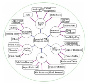
Factors influencing PCB manufacturing costs span the entire design and production process.
During the design phase, fundamental factors include PCB dimensions, layer count, materials, and complexity.
PCB size and layer count form the basis for cost calculation, directly impacting material consumption and processing time.
Typically, increasing the number of layers causes costs to rise exponentially.
Material costs account for over 25% of bare board expenses, where both consumption volume and material type are critical.
High-performance substrates carry significantly higher prices than standard substrates.
Therefore, if standard substrates meet performance requirements, there is no need to select high-performance ones.
Even when localized signal layers require high-frequency or high-speed capabilities, designers can adopt a hybrid structure that combines high-performance and standard substrates to reduce costs.
PCB complexity factors—such as routing density, hole types and aspect ratios, surface finish types—all impact costs.
High-density interconnect (HDI) laminations, plated-through holes with cover plating, and buried components all involve manufacturing cost factors.
PCB manufacturing requires advanced technology and expertise, and every operational step generates costs.
Figure 1 illustrates the breakdown of factors that influence costs.
Therefore, designing PCBs to simplify and optimize the manufacturing process aims to reduce production costs, enhance product quality and DFR, and shorten new product time-to-market.
In practice, PCB design must consider several factors.
Designers need to evaluate whether the substrate performance degrades.
They must also assess whether board thickness and copper foil can be reduced and whether dimensional tolerances can be increased.
Designers should also assess whether they can enlarge connection pad ring widths, use non-precious metals for surface finishes, and relax cosmetic defect requirements without compromising functionality.
Additionally, they must determine if meeting only Class 1 (low) standards is sufficient, without pursuing Class 2 (medium) or Class 3 (high) standards.
If PCB performance requirements exceed practical value, it constitutes design waste.
-
Communication Between Designers and Manufacturers Should be Integrated Throughout the Entire PCB Design Process.
Designers must incorporate DFM throughout the entire PCB design process.
From setting PCB structural dimensions and substrate selection to circuit layout and surface finishing, all aspects must consider manufacturability.
Therefore, when initiating a new PCB product design, designers must understand the manufacturer’s capabilities, including technical proficiency and delivery timelines.
They must also maintain communication with manufacturing engineers throughout the design process.
Simultaneously, PCB manufacturers and assemblers must be aware of the PCB product’s performance characteristics and comprehend the designer’s intent.
Communication between design and manufacturing teams enables timely correction of inappropriate design elements.
Designers integrate DFM throughout the entire process, from initial design to prototyping and trial production, to facilitate the joint resolution of complex issues.
The core of successful DFM lies in collaboration.
It results from continuous two-way communication and strategic cooperation, ultimately ensuring the seamless transformation of digital design files into physical boards.
Modern communication and transportation facilitate seamless interaction between parties.
However, the critical issue lies in information access and confidentiality, which depend on the trust built through long-term collaboration and the signing of non-disclosure agreements.
Yet, confidentiality should never be used as an excuse to neglect communication, as this could lead to unnecessary complications or even the failure of the partnership.
Design Document Integrity
Design documents record all requirements for PCB products specified by designers, conveying design intent to manufacturers through documentation.
Manufacturers produce PCB products in accordance with these design documents, ensuring products meet customized specifications.
-
Design File Principles
First, design and manufacturing parties must use consistent file formats or ensure mutual convertibility.
For many years, Gerber format has been the primary file format provided by PCB designers to manufacturers.
Newer formats like ODB++ and IPC-2581 are now also used, offering functional advantages.
Design files should output graphics data in a single format. Sending multiple versions leads to data inconsistencies and increases verification workload for manufacturers.
Second, design files must be complete and clear. Each file (drawing) should have a unique number and title, with PCB drawings assigned exclusive numbers.
Designers must display revision statuses after each number to track modifications.
Engineers provide a file inventory for each project to ensure a smooth handover to manufacturers and enable production strictly according to the drawings.
Furthermore, design file content must maintain consistency and uniformity.
When multiple subfiles within a complete set address the same subject, conflicting requirements are unacceptable.
For instance, differing dimensional tolerances or line width/spacing annotations for the same location across subfiles will cause confusion during manufacturing.
-
Requirements for Design Document Content
PCB design documentation encompasses a comprehensive set of files.
These range from circuit schematics (logic diagrams) and the bill of materials (BOM) to component placement layouts, PCB dimensional drawings, and PCB assembly and testing specifications.
From a PCB manufacturing perspective, the required design files include: The number of drawings varies based on PCB layer count and complexity.
The layout master file includes the PCB’s outline dimensions and all supporting details, such as substrate type, number of layers, and final surface finish.
It also contains product standards, grades, and necessary annotations to clearly convey the design intent.
Additionally, it includes all details not specified in other documents for board fabrication.
These details cover substrate safety (Underwriters Laboratories, UL) rating, copper type and thickness, solder mask thickness and color, and whether character markings are conductive.
The dimensional drawing indicates the PCB’s outline (length, width, thickness), the location and dimensions of critical holes or slots, and permissible tolerances.
For simpler PCBs, engineers incorporate the dimensional drawing into the main drawing (layout overview). For more complex PCBs, they may also use a netlist file for the dimensional drawing.
This file sets the coordinate positions of each hole, pad, and trace node according to the network format, facilitating manufacturing process setup and inspection corrections.
Graphic files use Gerber format, ODB++ format, or other formats mutually agreed upon by both parties, suitable for photoplotting output in PCB manufacturing.
Files include the solder mask and characters or other additional overlay graphics on the conductor pattern surface of each layer (outer and inner layers).
NC drilling and routing files provide detailed position and size information for each hole and slot requiring machining.
Drilling files are typically in Excelon format or other formats supporting numerical control (NC) machining.
Engineers present PCB bare board test information in a single file.
This file includes circuit connectivity networks that match the schematic and test sections with specific requirements, such as inductive impedance.
Where necessary, engineers must manufacture quality consistency test boards (attached test boards) simultaneously with the main board using the graphic files.
With the advancement of digitalization and intelligent manufacturing, design data files (non-traditional document packages) are directly output from electronic computer-aided design (eCAD) systems.
Engineers transmit these files to selected manufacturers, who automatically load them into their engineering or computer-aided manufacturing (CAM) systems.
Tools and production systems operate without human intervention, achieving zero-contact data transfer.
While design file transmission methods evolve, the fundamental requirements for manufacturability remain unchanged.
The perfection of the final PCB hinges on the perfection of the design files.
Material Selection
-
Material Selection Principles
1. Select only materials directly related to the performance of the finished PCB
Engineers categorize PCB materials based on their role in the product into physical/chemical materials and non-physical/chemical materials.
Physical/chemical materials refer to those applied during PCB production and constitute part of the finished PCB, such as copper-clad laminates and solder mask.
Non-physical/chemical materials refer to those applied and consumed during PCB production, such as photoresist dry films and chemical etchants.
Designers must explicitly specify physical materials in the design documents. Manufacturers determine non-physical materials based on the PCB processing conditions.
2. Select materials that meet performance requirements rather than the most expensive ones
PCB materials (physical and chemical materials) come in a wide variety. Material selection should prioritize technical performance that meets PCB product requirements.
Next, consider the material’s processability, opting for materials that facilitate production.
Finally, evaluate material cost, aiming for cost-effective solutions.
The fundamental principle is suitability and applicability—avoid blindly pursuing high performance, as expensive materials are not necessarily the optimal choice.
3. Select only readily available materials with ample supply
Given the vast variety of materials and complex supply chain channels, less common materials may face shortages or extended procurement cycles.
Therefore, avoid “obscure” materials whenever possible.
When discussing materials with manufacturers, designers should specify only the performance requirements.
This allows manufacturers to select detailed specifications and grades, expediting the procurement of suitable materials.
Substrate Materials
Substrate materials refer to copper-clad laminate (CCL), insulating adhesive (prepreg or adhesive film), copper foil, and other materials.
The substrate materials determine the fundamental properties of a PCB, including mechanical strength and electrical characteristics.
Traditional subtractive PCB manufacturing primarily relies on CCL as the core material.
The constituent organic resins, reinforcing fibers and fillers, and copper foil determine the performance of CCL.
For rigid PCBs, common CCLs include phenolic paper-based CCL and epoxy glass cloth CCL; for flexible PCBs, typical CCLs include polyester CCL and polyimide CCL.
As PCB performance requirements become increasingly complex, they place corresponding special demands on substrate material properties.
For instance, to meet high-frequency and high-speed transmission demands, PCB substrate materials require low dielectric constants and low dielectric losses.
Resin systems have evolved from modified epoxy and modified polyimide to polytetrafluoroethylene (PTFE), polyphenylene ether (PPE), liquid crystal polymers (LCP).
Glass fiber cloth reinforcements also reduce dielectric constant through weave pattern modifications, while copper foil roughness reduction minimizes skin effect.
To meet thermal conductivity and thermal stability requirements, engineers also employ additive or semi-additive processes for metal substrates, ceramic substrates, and other materials surrounding HDI boards, ultrahigh-density interconnect (UHDI) boards, and packaging substrates.
The focus lies on laminate materials—specifically insulating adhesives (bonding films)— with materials shifting from prepreg glass cloth to non-glass-reinforced resin media like resin-coated film (RCF) or resin-coated copper foil (RCC).
Achieving the right balance between material performance, sourcing, and cost ensures optimal selection.
-
Surface Materials
1. Solder Mask
The solder mask on PCB surfaces primarily serves three functions:
① Effectively prevents solder from entering non-soldering areas, reducing solder consumption and preventing solder bridging short circuits, while withstanding high-temperature processes like wave soldering and reflow soldering;
② Protects the board surface from damage, including scratches, oxidation, and contamination caused by physical and chemical hazards, requiring sufficient hardness and chemical resistance;
③ Enhances aesthetics and serves as a protective color. Solder mask (ink) offers diverse color options, with green being the most visually soothing and widely adopted.
Other colors (red, yellow, blue, black, white, colorless transparent) may be selected based on final product requirements.
For example, white solder mask is used on PCBs for LED lighting to enhance reflection.
Manufacturers generally do not strictly specify solder mask thickness.
However, designers must consider the dielectric constant and dielectric loss of the solder mask material, as well as the impact of its thickness, to minimize signal loss.
Flexible printed circuit boards (FPCBs) predominantly use cover films (insulating films of the same type as the substrate) as protective layers, with some employing solder masks.
Their additional property is the ability to flex and bend.
2.Character Marking
Character markings on PCB surfaces serve for product category identification, traceability, and component location identification.
Manufacturers print them using organic resin inks suitable for screen printing or inkjet printing.
Colors should contrast with the solder mask for easy recognition—e.g., white or yellow characters on green solder mask, black characters on white solder mask.
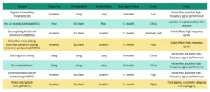
3.Final Finish
Manufacturers apply the final finish layer to cover the exposed copper conductor connection pads.
Its purpose is to protect the copper surface from oxidation, maintain good solderability or crimpability, and ensure low contact resistance.
Currently, the market offers multiple final finish options, each with its own advantages and disadvantages. Table 1 summarizes the key distinctions.
4.Other Materials
Certain PCBs have special requirements necessitating specific materials.
For example, if the PCB surface requires shielding or enhanced thermal conductivity, engineers should apply conductive or thermally conductive coatings or film materials.
To enhance bending strength, reinforced laminates should be used.
For PCBs incorporating buried components or embedded metal blocks, designers must also specify the corresponding component types and material specifications.
-
PCB Material Layer Annotation
The PCB layer stackup diagram specifies the fundamental information for each layer (layer number, material, thickness, type, and Gerber or file number), as shown in Figure 2.
This ensures consistent documentation throughout the design and enhances identification efficiency.
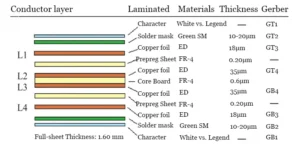
The laminate structure should maintain symmetry as much as possible, including the number of layers, dielectric thickness, copper foil thickness, and circuit pattern density.
Each layer should utilize the same prepreg and copper foil thickness whenever possible.
Engineers use hybrid materials in high-frequency PCBs to reduce costs.
When selecting a hybrid structure, comprehensively consider factors such as glass transition temperature (Tg), coefficient of thermal expansion (CTE), dimensional stability, and manufacturing process compatibility.

