The Functional Failure Analysis Case Study of PCBA Caused by HDI Blink Hole Defects
With the rapid advancement of microelectronics technology, electronic products continue to evolve toward lighter, thinner, shorter, and smaller designs.
With the rapid advancement of microelectronics technology, electronic products continue to evolve toward lighter, thinner, shorter, and smaller designs.
Aerospace electronic and electrical equipment continuously faces erosion from special environmental factors such as humid heat, mold, salt spray, and corrosive gases during service.
Printed circuit boards (PCBs) provide interconnections for electronic components and parts, forming modules or finished products with specific functions.
The principle of acid etching relies on the reaction between divalent copper in the etching solution and the metallic copper on the surface of the printed circuit board (PCB).
PCB warping is a critical issue in modern electronics manufacturing, particularly on automated surface mount lines, where even slight deformation can cause misalignment, poor component placement, or damage to insertion machinery.
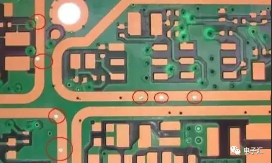
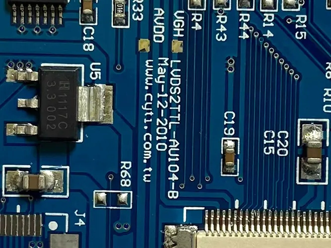
Via holes serve to interconnect circuit traces. The advancement of the electronics industry has driven the development of PCBs while imposing higher demands on printed circuit board manufacturing processes and surface mount technology.
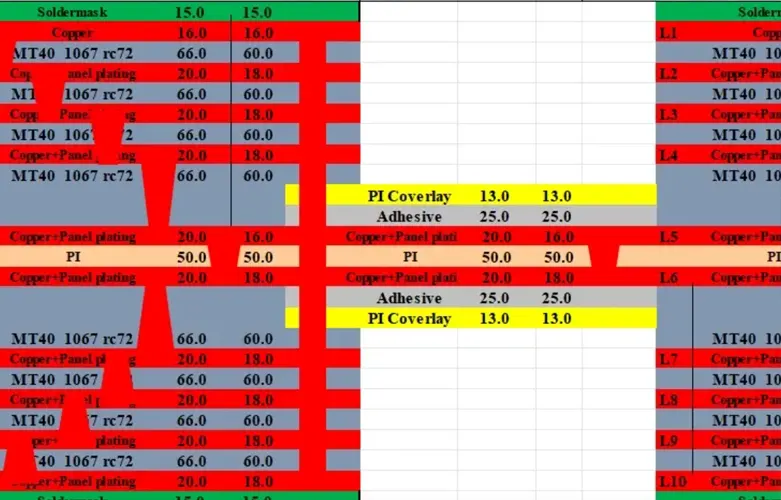
As the functionalization of multilayer printed circuit boards (PCBs) continues to advance, multilayer PCBs are often designed with stepped structures featuring varying board thicknesses.
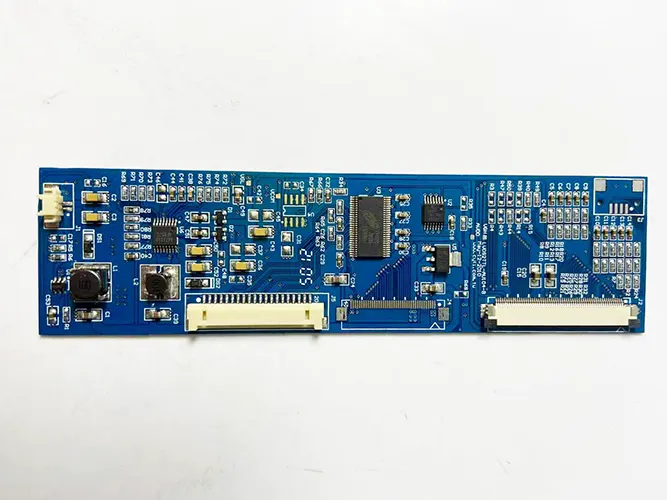
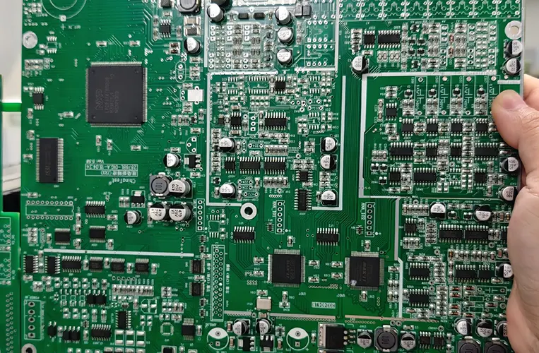
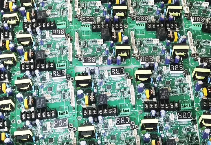
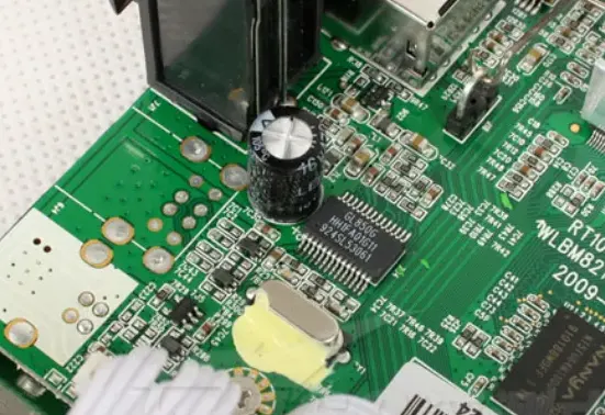
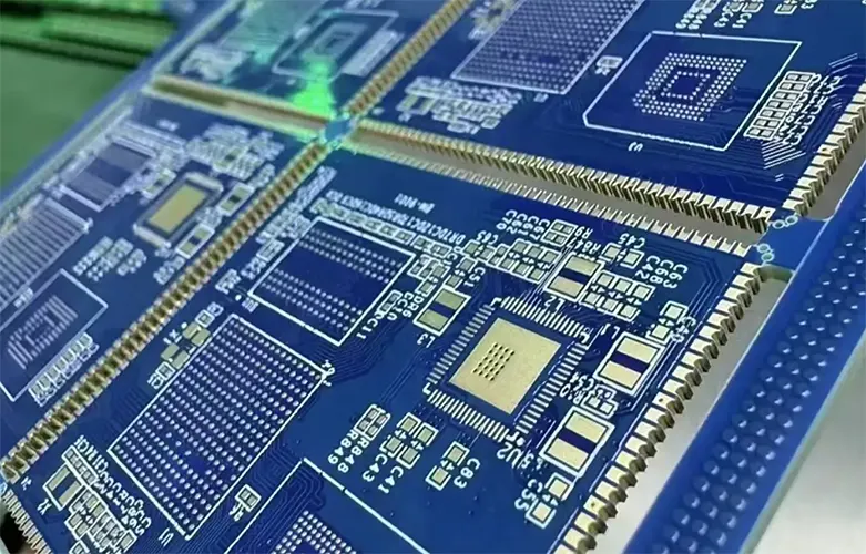
Printed Circuit Board Assembly (PCBA) consists of a Printed Circuit Board (PCB), electronic components, and structural elements, assembled through precision soldering and mounting processes.
In the era of rapid advancements in communication technology, terminal application scenarios are becoming increasingly diverse and undergoing continuous iteration and renewal.
Printed circuit boards (PCBs) serve as fundamental components of electronic products, playing a crucial role in contemporary technology. With the advancement of 5G technology, communication systems demand ever-increasing speeds and capacities, thereby imposing stricter specifications on PCB substrate characteristics such as thickness, surface morphology, and impedance.