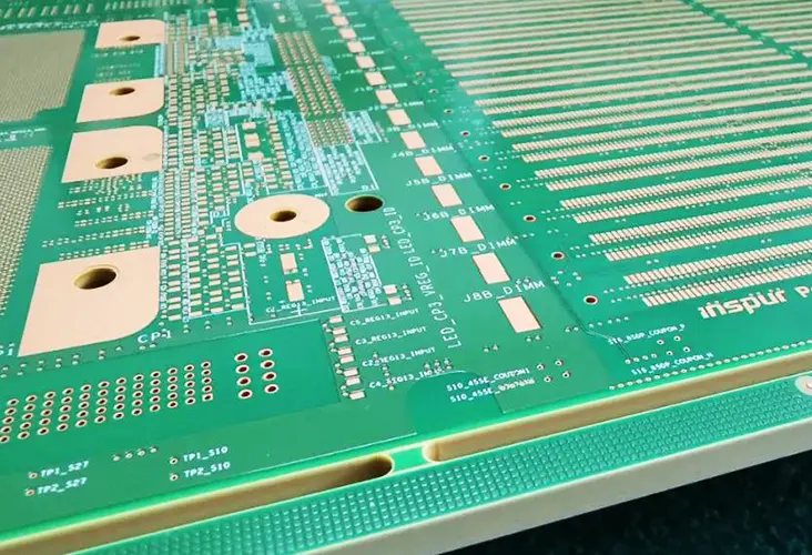
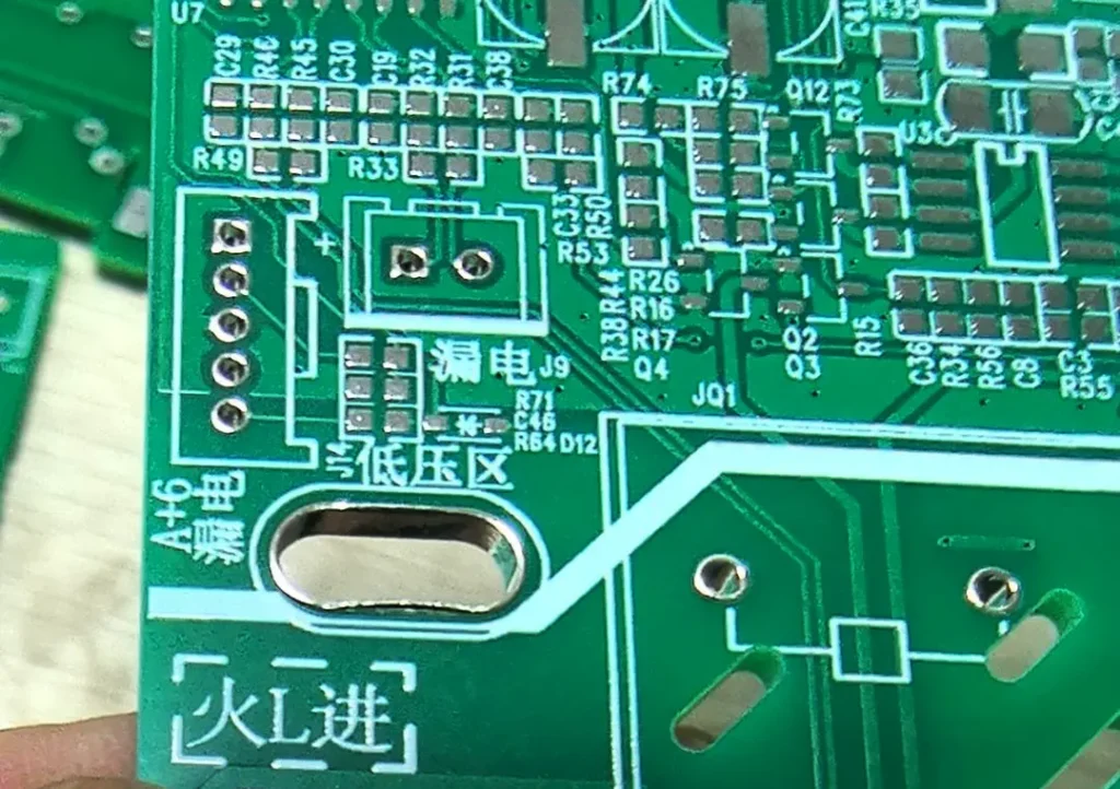
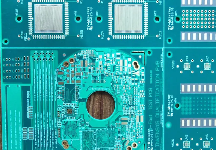
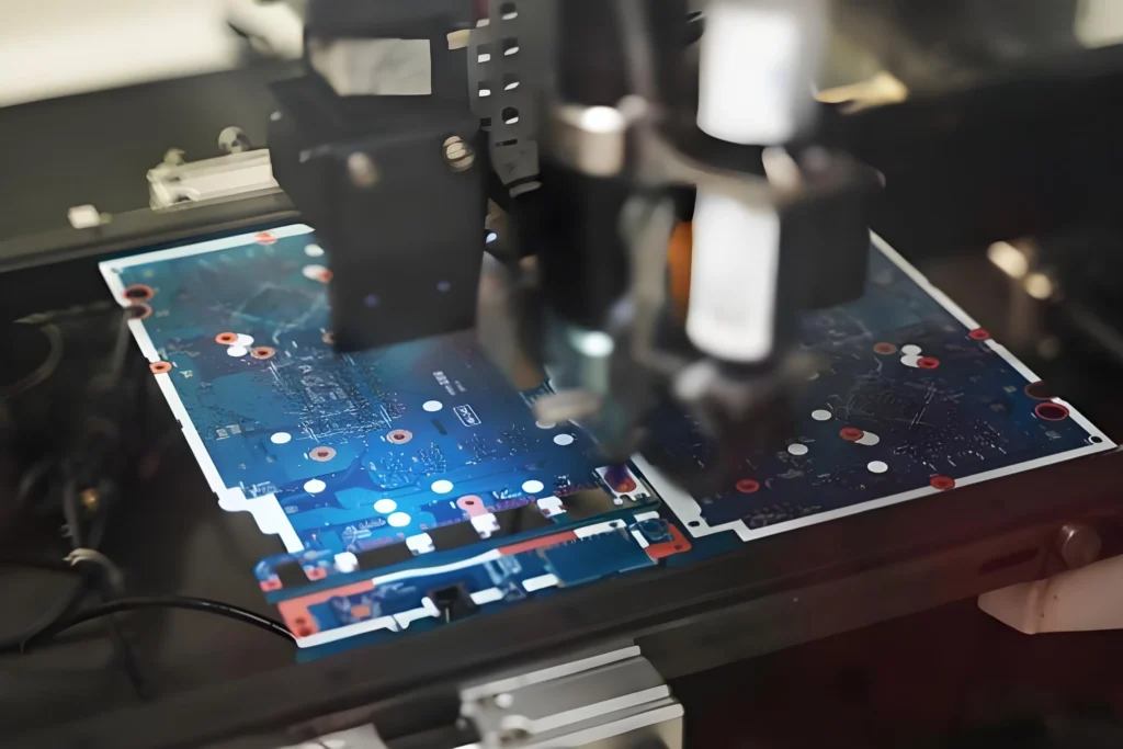
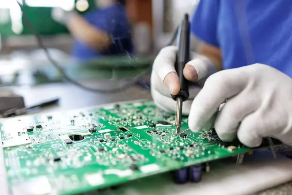
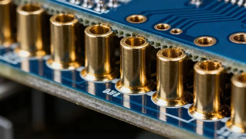
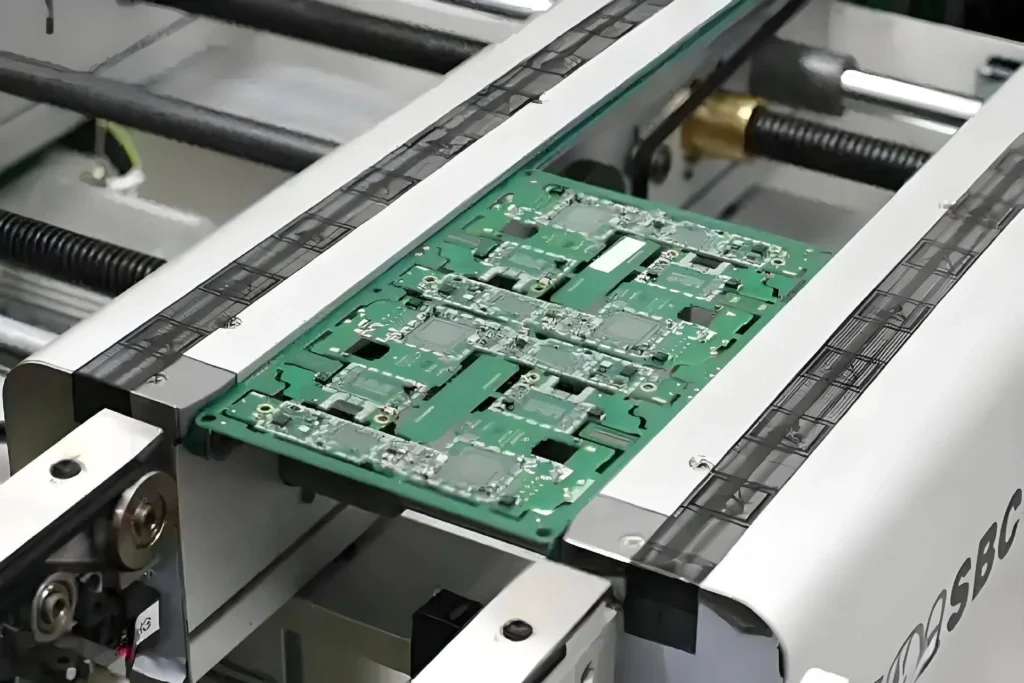
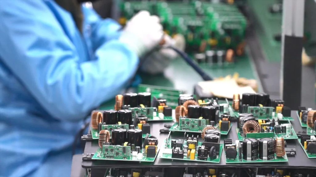
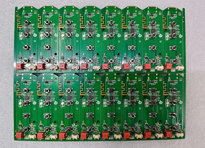
Blog

Featured Image

PCB Design: Relationship Between Current and Trace Width

Numerous empirical formulas, correlation tables, and software tools regarding PCB trace width and current are available online. The following summarizes eight different formulas, tables, and calculation methods for the relationship between current and trace width.

pcb manufacturing

What is a stepped slot in PCB manifacturing? How is it made?

PCB step slots, also known as controlled-depth slots or non-through slots, are recessed grooves milled into specific layers within a PCB board without penetrating the entire board. Imagine them as “pits” dug between the “floors” of the PCB.

Featured Image

Layer Stackup Planning for RF Circuit Boards

When designing multilayer circuits requiring impedance control, printed circuit board (PCB) designers must collaborate closely with engineers experienced in radio frequency (RF) PCB layout, including mixed-signal application specialists.

Featured Image

Further Explore SMT Process Control

As living standards continue to rise, increasingly stringent demands are being placed on the soldering reliability of electronic products across all sectors. The entire industry is conducting ever more detailed research into the depth and breadth of electronic assembly and smart manufacturing.

Featured Image

Erection Monument Defects in SMT: What Causes Them and How to Fix Them

Currently, global electronic products are progressively evolving toward multifunctionality, intelligence, integration, and miniaturization. As electronic devices gain more functions while printed circuit boards (PCBs) offer limited spatial layout, surface mount technology (SMT) has become the mainstream electronic assembly technique.

Scroll to Top