With the explosive growth of the AI computing power industry and the rapid adoption of new energy vehicles, the power density of electronic devices is increasing steadily.
This places far greater demands on PCB thermal management and structural strength than traditional products can meet.
As a high-end specialty PCB specifically designed to address these industry pain points, copper-embedded PCBs are becoming a hot product in the high-end electronics sector.
Today, we’ll take a detailed look at the core advantages of copper-embedded PCBs.
Superior Heat Dissipation Performance
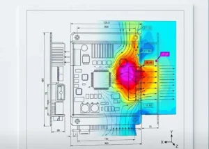
Against the backdrop of the rapid proliferation of high-power electronic devices, the power consumption of components such as high-power ICs, IGBTs, CPUs, and GPUs has exceeded one kilowatt.
Heat rapidly concentrates in localized areas, and if it is not dissipated promptly, it can easily lead to component overheating and failure.
Traditional heat dissipation solutions—such as drilling heat-dissipation holes or attaching external heat sinks—either have low thermal conductivity or occupy additional design space, making it difficult to meet the demands of high-power-density applications.
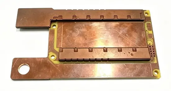
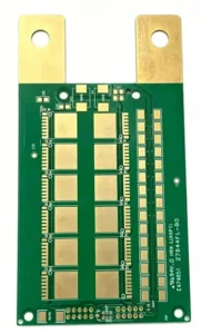
Copper-embedded PCBs incorporate a high-purity solid copper block directly beneath the heat-generating components.
Copper has a thermal conductivity of approximately 400 W/m·K—far higher than the thermal conductivity of the FR4 substrate, which is less than 0.3 W/m·K—providing a direct, low-thermal-resistance pathway for heat to rapidly dissipate from the heat source.
Compared to standard thick-copper-foil PCBs and aluminum substrates, copper-embedded PCBs can improve heat dissipation efficiency by 3 to 5 times.
The copper block not only makes direct contact with the heat source but can also be connected to heat sink pads on the other side of the PCB, an external heat sink, or other heat dissipation layers via thermal vias designed within the copper block, further enhancing thermal conductivity.
This fundamentally resolves the issue of excessive localized temperature rise in high-power devices.
Whether in GPU modules for AI servers or power devices in new energy vehicles, embedded copper PCBs can keep device junction temperatures within a reasonable range, significantly improving operational stability.
Enhancing Structural Strength
Many PCBs are equipped with heavy components, such as large connectors, high-power transformers, and large inductors.
If these components rely solely on the PCB substrate for support, the solder joints are prone to breaking due to vibrations and impacts during equipment handling, which can lead to equipment failure.
This issue is particularly pronounced in fields such as automotive electronics and industrial control, where equipment is frequently subjected to complex operating conditions.
Copper-embedded PCBs incorporate solid copper blocks beneath the components, providing additional mechanical support for these heavy-load components.
This significantly enhances the solder joints’ impact resistance and prevents premature failure.
In addition to supporting heavy components, copper-embedded PCBs can also enhance local rigidity.
In areas subject to frequent insertion and removal—such as gold fingers and board-edge connectors—embedded copper blocks increase local strength, preventing the PCB from breaking or deforming during these operations.
For large, multilayer PCBs, locally embedded copper blocks also improve the board’s overall resistance to bending, reducing the rate of deformation during transportation and assembly, and thereby enhancing product yield and long-term reliability.
Increasing Current-Carrying Capacity
With the widespread adoption of 800V high-voltage platforms in new energy vehicles, as well as the development of high-power energy storage converters and industrial inverters, PCBs are required to carry increasingly higher currents.
Conventional PCBs rely on copper foil for conductivity; however, the thickness of copper foil is limited, and its cross-sectional area is small.
When high currents flow through it, significant resistance is generated, which not only results in additional energy loss but also produces more heat, further increasing the temperature rise of the entire system and posing potential risks to equipment operation.
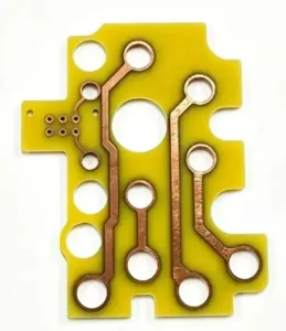
The solid copper blocks in copper-embedded PCBs have a cross-sectional area far greater than that of standard copper foil.
With extremely low resistance, they can carry very high currents while generating minimal heat themselves, making them perfectly suited for high-current applications.
Copper blocks in copper-embedded PCBs are frequently used in power supply input and output paths, as well as at ground plane connection points.
In addition to carrying high currents, they reduce power loss during conduction and improve the overall energy efficiency of the system.
For high-power equipment that requires prolonged operation, even a few percentage points of improved energy efficiency can result in significant savings on electricity costs over the entire lifecycle.
This not only meets the environmental requirements of the “Dual Carbon” goals but also reduces users’ operating costs and enhances the product’s overall competitiveness.
Optimizing Shielding and Grounding
Today’s electronic devices not only operate at increasingly higher power levels but also feature ever-faster signal frequencies.
The SerDes transmission rates of AI servers have already exceeded 224 Gbps, while RF power amplifier products operate at frequencies as high as the GHz range.
Electromagnetic interference (EMI) between different modules is becoming increasingly severe, easily leading to signal distortion and increased bit error rates, which can affect the normal operation of the equipment.
Solid copper blocks embedded in copper-embedded PCBs can serve as excellent local grounding points or electromagnetic shields, effectively blocking electromagnetic crosstalk between different modules and optimizing signal transmission quality.
For products such as high-frequency, high-power amplifiers and 5G communication base station RF modules, high-quality local grounding and shielding can significantly improve the signal-to-noise ratio, reduce the impact of external interference on signals, and enhance the communication quality of the equipment.
In high-density integrated modules, embedded copper shielding achieves excellent shielding performance without occupying additional external space, enabling a more compact design without sacrificing shielding performance—making it an ideal choice for high-frequency, high-density equipment.
Suitable for Compact Designs
Today, consumer electronics and computing devices are trending toward miniaturization and high integration.
As a result, the space available for thermal management systems within the device is becoming increasingly limited.
Traditional external heat sinks occupy additional space on the PCB surface, which not only restricts component layout but also increases the overall thickness of the device, failing to meet the demands of compact design.
Copper-embedded PCBs incorporate copper blocks into the interior or surface layer of the PCB, forming an integrated structure with the PCB itself.
This eliminates the need to install additional heat sinks on the PCB surface, saving surface layout space and enabling a more compact design that meets the demands of miniaturized, highly integrated products.
Compared to copper-based PCBs made entirely of metal, copper-embedded PCBs embed copper blocks only in specific areas requiring heat dissipation.
This approach achieves excellent thermal performance while avoiding the high cost and weight associated with using copper across the entire board.
Additionally, copper-embedded PCBs can be manufactured as multilayer boards, balancing the ability to route precision circuits.
They are suitable for applications that require both high-density wiring and stringent thermal management, such as power boards for AI servers and in-vehicle control boards, perfectly balancing routing density and thermal management needs.
Reducing Total Life Cycle Costs
Many people’s first impression of copper-embedded PCBs is that their initial purchase cost is higher than that of traditional PCBs.
In fact, from a full life cycle perspective, the total cost of copper-embedded PCBs is actually lower.
According to industry estimates, in applications with a power density of 20 kW or higher, although copper-embedded PCBs have an initial cost that is 45% to 60% higher, their total cost of ownership over the full life cycle can actually be reduced by 22% to 28%.
When the power per cabinet exceeds 15 kW, and the equipment’s service life exceeds 4 years, copper-embedded PCBs already offer a clear cost advantage.
Copper-embedded PCBs can lower the junction temperature of chips, and the lifespan of semiconductor devices is closely related to junction temperature;
Generally, for every 10°C reduction in junction temperature, the device’s lifespan can be roughly doubled.
At the same time, copper-embedded PCBs reduce the number of external heat dissipation components, thereby lowering the probability of failures in these components.
This further reduces the equipment’s failure rate and lowers maintenance costs during operation and maintenance.
For sectors such as data centers and new energy vehicles—which demand high reliability and have long service lives—the benefits derived from lower failure rates and longer service lives far outweigh the initial cost premium.
Compatibility with Existing Processes
Many original equipment manufacturers (OEMs) worry that, as a specialty PCB, copper-embedded PCBs might require additional adjustments to their existing production and assembly processes, thereby increasing development and production costs.
In fact, once copper-embedded PCBs are manufactured, their assembly requirements are no different from those of standard PCBs.
They are fully compatible with conventional SMT assembly processes, requiring neither modifications to existing production lines nor additional assembly steps.
This significantly lowers the barrier to entry for OEMs and reduces both product development costs and time-to-market.
After years of development, the manufacturing process for copper-embedded PCBs has become highly mature.
The industry is now capable of stably mass-producing copper-embedded PCBs of various specifications, with copper blocks as small as 3 mm, board thicknesses ranging from 0.4 mm to 6.5 mm, and flatness controlled to within ±0.025 mm.
They also pass various reliability tests, including thermal shock, reflow soldering heat resistance, and dielectric withstand voltage, meeting automotive-grade and industrial-grade requirements.
Most reputable high-end PCB manufacturers can provide stable mass production services without lengthy customization lead times, fully meeting the demands of large-scale mass production.