Currently, global electronic products are progressively evolving toward multifunctionality, intelligence, integration, and miniaturization.
As electronic devices gain more functions while printed circuit boards (PCBs) offer limited spatial layout, surface mount technology (SMT) has become the mainstream electronic assembly technique.
It enables the combination of short, small, light, and thin discrete discrete components with varying performance characteristics and high-density PCBs.
While SMT technology is relatively mature, its manufacturing process involves multiple steps. Common defects may arise during actual production.
This article briefly introduces the “tombstoning” defect and provides corresponding solutions to help improve SMT placement production quality and efficiency while reducing manufacturing costs.
The “Standing Monument” Phenomenon and Its Hazards
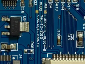
During reflow soldering in SMT production, uneven stress distribution causes components to tilt or flip, resulting in discrete surface-mount devices standing upright at one end or lifting at both ends, as shown in Figure 1.
When one end of a component lifts off the pad while the other remains incompletely soldered, this is commonly referred to as the “standing monument” phenomenon.
This defect can cause solder joint open circuits or short circuits, resulting in electrical performance failure and consequently affecting circuit functionality.

Analysis and Solutions for “Tombstoning” Defects in SMT Soldering
-
Addressing Tombstoning Through Design
1.Pad Design
(1) Improper Pad Design
Pad design is a critical aspect of PCB layout.
It not only determines the soldering position of surface-mount devices (SMDs) on the printed circuit board but also significantly impacts solder joint reliability, potential “tombstoning” defects during soldering, testability, visual inspection, and maintenance.
For small discrete components, designing pads of different sizes at opposite ends may cause the component to stand upright.
When one pad is significantly larger than the other, this is the primary cause of the “standing” effect.
(2) Optimizing Pad Design
Symmetry Design: PCB pad dimensions and shapes must be strictly symmetrical, adhering to the IPC-7351 standard (e.g., recommended 0.5mm spacing for 0402 component pads).
Pad Spacing Adjustment: Avoid excessive spacing that causes component suspension or insufficient spacing that leads to solder paste bridging.
SMT pad and design requirements are illustrated in Figure 2 and summarized in Table 1.


2.Pad Connection and Trace Design
(1) Improper Pad Connection Trace Gesign:
Unequal conductor areas in pad connection traces cause one end to heat up too quickly during soldering, resulting in differing melting times at both ends and potentially causing component “tombstoning.”
For example, if one pad end connects to ground or power with a large ground area, the increased thermal mass at that end leads to uneven heating across the component.
Alternatively, if one pad has a ground via, the via can cause solder loss, reducing surface tension.
This also leads to uneven stress distribution and increases the likelihood of tombstoning.
(2) Solution: Thermal Balance Design
Implement “thermal isolation” for high-thermal-conductivity pads (e.g., reducing trace width or adding thermal break grooves).
The adjusted trace-to-pad connection method is shown in Figure 3.

3.Reference Mark Design
(1) Reference Mark Design Defects
Reference marks serve as optical positioning guides for solder paste printing and component placement.
They provide common measurable points for all steps in the SMT assembly process.
Asymmetrical or insufficiently precise placement reference marks cause component misalignment.
During high-volume production, they ensure every assembly device can accurately position circuit patterns.
(2) Solution: Properly Designing Reference Points
① Reference Point Composition: A complete reference point consists of a positioning point (also called a marking point) and an open area.
② Reference Point Shape: The preferred shape is a solid circle.
③ Reference Point Dimensions: The preferred diameter is 1.0mm, with a maximum diameter of 3.0mm.
It is particularly important that all reference points on the same PCB board number must be of consistent size.
④ Solder Mask Opening for Reference Points: The solder mask opening should be a circle concentric with the reference point, twice the diameter of the reference point.
A protective copper ring with a line width of 0.2mm is required along its edge.
⑤ Reference Point Placement:
a. Each assembly unit board must have at least two asymmetrically positioned reference points (to prevent misassembly), distributed along the longest diagonal or one at each of the three corners: For large-sized or high-precision components like dual flat packages (DFP), chip-scale packages (CSP), or ball grid array packages (BGA), local reference points should be placed at the diagonals or center positions.
b. The edge of the reference point should be at least 5mm from the PCB board edge and protected by a metal ring.
⑥ Clearance Zone Requirements Around Reference Points: To ensure recognition accuracy by printing and placement equipment, maintain a clear area free of screen printing, printed conductors, pads, or V-groove cuts around reference point markings.
The radius r of this clearance zone must be ≥2R (where R is the reference point radius). A radius of r ≥3R yields optimal machine recognition performance.
-
Resolving “Tombstone” Issues Through Process Factors
1.Stencil and Placement Offset
Typically, stencil misalignment during placement, coupled with variations in printing force and direction, causes minor displacement of smaller surface-mount components.
During reflow soldering, surface tension from molten solder paste automatically corrects this displacement—a phenomenon termed “self-adaptation.”
However, excessive offset can cause the solder pull to “stand up” the component, resulting in tombstoning.
Root Causes: Poor repeatability of the printing machine, placement misalignment (due to inaccurate stencil registration, PCB misalignment, improper stencil aperture, or printing parameters), leading to solder paste printing beyond the pad.
Uneven solder paste distribution causes solder terminals with greater contact area to absorb more heat capacity and melt first.
Mismatched stencil aperture size and thickness design causes excessive solder paste, resulting in differing adhesive forces between the device terminals and solder paste during heating.
Solutions: Prepare thinner stencils before printing. Carefully inspect font size, line thickness, patterns, positional dimensions, broken lines, deformation, or damage on the stencil.
Check each substrate’s pad metal layer for contamination, oxidation levels, and foreign objects. Ensure no foreign objects are present and avoid direct hand contact with PCBs.
Wear anti-static gloves and adjust the placement accuracy of the printing machine.
Position the substrate correctly within the printer.
Based on the printer’s programmed settings, the placement machine can calibrate by manually or automatically locating reference points, ensuring precise circuit pattern alignment for each assembly device.
After printing, carefully inspect the printed quality.
2.Furnace Temperature Profile Control
Uncontrolled reflow temperature profiles, uneven preheating, or excessively high peak temperatures exacerbate thermal stress differences between the two ends.
After component placement, place the PCB into the reflow oven for soldering.
Before passing through the oven, test the preheating zone using a test board: control the heating rate at 1–3°C/s to minimize thermal shock.
The obtained curve should be a thermal profile with an extremely slow heating rate.
When producing the first side (bottom), place the PCB on the reflow oven’s mesh tray for processing.
Reflow stage: Peak temperature is recommended at 235–245°C for 40–70 seconds to ensure simultaneous solder paste melting at both ends.
When producing the second top side, the PCB must be placed on the track for reflow. When using the track, verify that it does not interfere with components on the PCB.
During the cooling zone phase, maintain a forced air cooling rate ≤4℃/s to prevent stress concentration caused by rapid cooling.
After passing through the reflow oven, conduct a visual inspection of the product.
Eliminate “tombstoning” to reduce soldering defects, enhance product quality, and achieve cost reduction and efficiency gains.
Conclusion
With the rapid advancement of artificial intelligence technology, the demand for low-cost, highly reliable electronic assembly products has become increasingly urgent.
While numerous factors influence soldering quality in SMT production, this article has focused solely on the common “tombstoning” defect in components.
To minimize or prevent other soldering defects, efforts must extend beyond optimizing PCB pad symmetry and thermal balance during design, and beyond controlling printing, placement, and reflow processes during manufacturing.
Strict production process control is essential.
Additionally, enhancing technicians’ ability to identify and resolve defects, refining management measures, and establishing and improving production workflows are crucial steps toward consistently producing high-quality electronic products.