
The greatest challenge in high-speed design is to minimize crosstalk as much as possible, ensure good signal integrity during transmission, and minimize the impact of noise on the circuit board.
Since single-ended signals and low-voltage differential signaling (LVDS) are typical types of high-speed interface signals, it is essential to ensure the reliable transmission of both.
Today’s article focuses on transmission line termination, minimizing crosstalk in signal channels, and circuit board-level filtering and decoupling.
Transmission Line Termination
Different termination methods:
Near-end (source-end) termination.
Far-end termination.
Proximal (Source-Side) Termination
Designers typically adopt this method for single‑ended lines in cases where the output‑driver impedance is lower than the transmission‑line impedance.
In such scenarios, designers add a series terminator at the driver output to match the transmission‑line impedance.
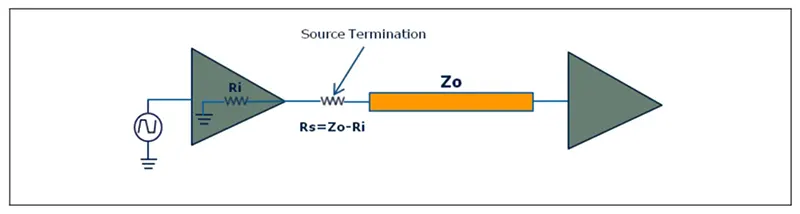
Place the resistor relatively close to the source driver.
When connecting point-to-point, use source-side termination.
Do not use a daisy-chain topology.
Designers must place all loads at the transmission‑line terminus.
Remote Termination
Parallel or AC termination is the most common method for remote termination of HSSI.
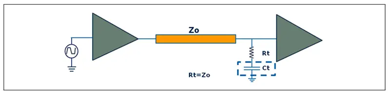
Designers shall match the parallel‑termination impedance to the transmission‑line characteristic impedance.
Because a DC path exists at the line terminus, parallel termination results in power dissipation.
When adopting parallel‑termination schemes, designers implement adequate thermal‑management measures.
AC termination avoids power dissipation by inserting a capacitor in series with the termination resistor.
The capacitance value for AC termination ranges from 100 to 200 pF.
Due to the capacitive load, this termination technique increases load rise and fall times.
Timing considerations must be taken into account when selecting different capacitance values.
Place the components near the receiver pins to eliminate the need for shorting wires.
Termination of Differential Lines
Special attention should be paid to the termination of differential lines.
Differential lines require a line impedance greater than 50 ohms and a differential impedance of 100 ohms.
Accordingly, designers set the termination impedance to 100 Ω.
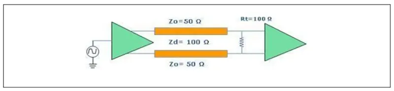
Place terminations after the traces connect to the receiver pins; this eliminates the need for a stub before the receiver.
This helps prevent reflections caused by impedance discontinuities.
When placing terminations, do not change layers or use vias.
Minimizing Crosstalk Between Signal Channels
When signal lines are routed in parallel over long distances, electrical coupling can occur.
Careful PCB design can help prevent such coupling issues:
Separate the routing layers for single-ended and differential signals.
If two adjacent layers contain high-speed lines, route all traces perpendicular to each other.
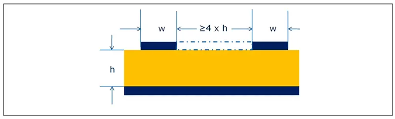
Do not route signal lines near a point that is four times the electrical height of the reference plane.
Minimize the distance to the reference plane as much as possible.
Transmission lines closer to the reference plane experience less coupling with adjacent lines.
Avoid routing high-speed signals in parallel over long distances.
For differential signals, maintain a constant spacing along the length of the traces.
When serpentine routing is necessary for differential‑pair length matching, designers set the spacing between parallel traces to four times the dielectric height.
Use serpentine routing on the transmitter side, not the receiver side, to achieve length matching.
Designers route critical signals on adjacent layers in orthogonal orientations.
PCB Level Filtering and Decoupling
Decoupling the power distribution network of a microcontroller IC is a critical step in the PCB design process, as the selection and placement of decoupling capacitors significantly impact the PCB’s high-speed performance and can reduce radiation.
On-board decoupling capacitors are effective in the 1 MHz–200 MHz range.
For frequencies above 200 MHz, use a power plane to act as a decoupling capacitor.
Designers determine the performance of decoupling capacitors through proper placement and correct interconnection.
Place capacitors as close to the microcontroller as possible.
Minimize the interconnection inductance between the MCU and the capacitor.
Use capacitors with low resistance and reactance (ESR and ESL).
Since parasitic inductance limits the capacitor’s response to device current demands at high frequencies, select the capacitor’s ESL and connection inductance to achieve optimal design performance.
Connect the capacitor via vias close to the pads.
Place the vias on the opposite side to minimize the current path.
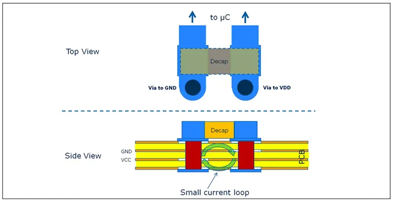
Use dual vias to reduce parasitic inductance.
When placing capacitors, optimize the solder area, trace routing, and vias.
Do not use long traces to connect capacitors to GND or VDD.
Always maintain a short high-frequency current return path (path of minimum reactance).
Select the smallest available package type for capacitors.
Select capacitor type: multilayer ceramic X7R or X5R.
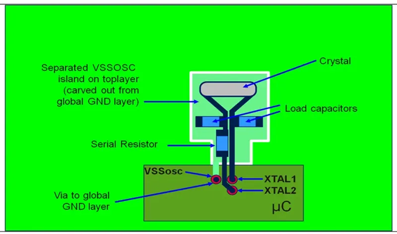
To reduce radiation/coupling from the oscillator circuit, create a ground island on the GND plane.
One point of the ground island connects to the GND plane.
The noise generated by the oscillator circuit is confined to this isolated ground island.
Designers route the VSSOSC ground connection for the load capacitor to the ground island.
The traces for the load capacitor and Xtal should be kept as short as possible.
To minimize EMI radiation from the PCB as much as possible, special attention should be given to the following key signals:
- LVDS pins (HSCT, MSC, QSPI, AGBT)
- ERAY pins
- Ethernet pins
- QSPI pins
- MSC pins
- External clock pins
- Power pins
Conclusion
In high-speed circuit development, reasonable transmission line termination, crosstalk suppression, and power network decoupling work synergistically to guarantee the transmission quality of single-ended signals and LVDS interfaces.
Designers need to select appropriate source-end or far-end termination methods for single-ended traces and strictly follow 100-ohm differential impedance matching rules for differential wiring.
Adhering to orthogonal routing, controlled trace spacing, and standardized serpentine length-matching rules effectively lowers crosstalk between signal channels.
In terms of power integrity, proper selection, compact placement, and low-inductance wiring of decoupling capacitors optimize high-frequency power supply filtering.
Additionally, targeted measures such as isolated ground islands for oscillator circuits and priority control of high EMI-risk signals help limit noise radiation.
Following these layout specifications comprehensively improves signal integrity and enhances the overall anti-interference performance of high-speed PCBs.
If you need, I can compress this pair of texts into shorter abstract versions suitable for engineering documents.

