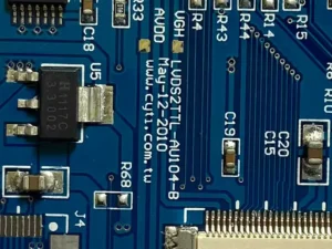
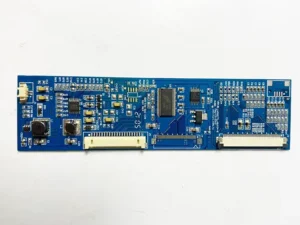
Copper-clad laminates (CCLs) are the foundational materials of printed circuit boards, providing both mechanical support and electrical functionality.
As the first material introduced into the PCB manufacturing process, their dimensional accuracy, electrical performance, and thermal stability directly determine downstream process capability and long-term product reliability.
Industry data indicates that more than 60% of modern electronic components incorporate threaded or laminated structures.
Within PCB manufacturing, base material-related defects account for a significant proportion of latent failures.
This white paper presents a structured, data-driven framework for inspecting and ensuring the quality of PCB base materials, incorporating industry standards, quantitative acceptance criteria, and application-specific risk controls.
Introduction
With the rapid advancement of electronics toward higher frequencies, faster signal transmission, and increased thermal loads, PCB base materials are required to meet increasingly stringent performance thresholds.
Beyond serving as passive substrates, modern laminates must maintain stable dielectric behavior, mechanical integrity, and thermal resistance throughout multiple processing cycles and extended service life.
Experience across the PCB industry shows that many failures observed during electrical testing or field operation originate from insufficient control at the laminate incoming inspection stage.
Thickness deviations, dielectric inconsistency, moisture sensitivity, or poor copper adhesion often remain undetected until irreversible processing steps have already occurred.
A quantitative and standards-based inspection methodology is therefore essential to minimize systemic manufacturing risk.

Inspection Standards and Sampling Strategy
Laminate inspection must be grounded in clearly defined technical references, including supplier datasheets, IPC-4101 specifications for rigid and multilayer PCB base materials, customer drawings, and internal quality standards.
Among these, IPC-4101 provides standardized classification of material types and minimum performance requirements, forming the baseline for technical acceptance.
Sampling strategies are commonly derived from MIL-STD-105E or GB 2828.1, with acceptance quality limits (AQL) selected according to risk level.
While statistical sampling is suitable for general appearance and dimensional checks, many manufacturers adopt 100% inspection or batch-level verification for critical parameters such as thickness and copper weight.
For first-time deliveries or supplier changes, inspection levels are typically tightened to mitigate variability risk before stable process capability is confirmed.
Visual and Structural Integrity Assessment
Visual inspection provides the first indication of laminate process stability.
The copper surface must be smooth and uniform, free from scratches, dents, wrinkles, pinholes, oxidation, or foreign contamination.
Even minor surface defects can compromise etching uniformity and reduce conductor reliability after thermal cycling.
The insulating substrate must exhibit complete structural integrity, with no bubbles, delamination, resin-rich spots, resin voids, fiber exposure, or white spotting.
Such defects are unacceptable, as they can lead to dielectric breakdown or mechanical failure under thermal stress.
Engineers also evaluate color consistency, particularly for FR-4 materials, which typically appear light yellow.
Within the same batch, they consider visible color variation an indicator of material inconsistency and potential performance deviation.
They examine panel edge quality to ensure clean, uniform cutting without excessive chipping, burrs, or layer separation, as poor edge integrity can initiate delamination during lamination or soldering.
Dimensional Accuracy and Thickness Control
Dimensional conformity is critical for automated PCB manufacturing.
Laminate length, width, and diagonal dimensions must meet purchase order requirements, with commonly accepted tolerances ranging from ±1.0 mm to ±2.0 mm, depending on panel size and application.
Thickness control is one of the most critical inspection parameters.
Engineers typically measure total laminate thickness using calipers or micrometers, ensuring it conforms to nominal values such as 1.5 mm ± 0.1 mm.
Beyond nominal compliance, thickness uniformity across a single panel is equally important. Engineers perform multi-point measurements and generally limit allowable intra-panel thickness deviation to ≤10% to ensure impedance stability and minimize the risk of warpage.
Copper foil thickness is verified based on nominal copper weight. For example, 1 oz copper corresponds to approximately 35 μm, with typical acceptance tolerances of ±10%.
Engineers may perform verification using copper thickness gauges or microsection analysis, particularly for impedance-controlled or high-current designs.
Electrical and Mechanical Performance Evaluation
Electrical performance verification becomes increasingly critical as operating frequencies rise. Dielectric constant (Dk) and dissipation factor (Df) directly affect signal propagation speed and insertion loss.
For high-frequency laminates, engineers treat these parameters as mandatory inspection items and measure them using dielectric resonator methods or vector network analyzers to ensure compliance with supplier specifications.
Engineers evaluate insulation integrity through surface and volume resistivity testing. Under standard environmental conditions, PCB base materials typically require resistivity values exceeding 10⁷ MΩ, ensuring sufficient resistance to leakage currents.
Dielectric withstand testing further validates material performance under elevated voltage stress, according to the material grade and intended application.
Mechanical performance assessments complement electrical testing. Copper peel strength reflects the bonding quality between the copper foil and the substrate, and engineers commonly evaluate it after thermal stress.
Typical acceptance criteria require peel strength values of ≥1.0 N/mm, ensuring adequate resistance to delamination during soldering and thermal cycling.
Flexural strength testing, performed in accordance with IPC-TM-650 2.4.4, provides insight into laminate rigidity and resistance to deformation.
Thermal and Environmental Reliability
Thermal reliability is a defining characteristic of modern PCB materials, particularly under lead-free assembly conditions. Glass transition temperature (Tg), measured using DSC or TMA, indicates the temperature at which material properties begin to change significantly.
Standard FR-4 materials typically require Tg ≥130°C, while medium- and high-Tg materials are specified at ≥150°C or ≥170°C for enhanced thermal robustness.
Thermal decomposition temperature (Td) reflects chemical stability at elevated temperatures. Engineers generally prefer Td values of 300 °C or higher, as these values provide sufficient margin against degradation during multiple reflow cycles.
Engineers assess resistance to solder immersion by exposing laminates to molten solder at 288 °C for 10 seconds. Under these conditions, the materials must remain free from blistering, delamination, or structural damage.
Engineers further evaluate environmental reliability through moisture absorption testing in accordance with IPC-TM-650 2.6.2, and they consider low water uptake values—typically below 0.2%—favorable for maintaining dielectric stability.
For high-density or high-voltage PCBs, resistance to conductive anodic filament (CAF) formation is also evaluated to ensure long-term insulation reliability under bias and humidity.
Material-Specific Considerations
Inspection priorities vary significantly by material type. High-frequency and high-speed laminates such as Rogers or Taconic materials require manufacturers to tightly control Dk and Df consistency, as well as copper foil roughness, with low-profile copper preferred to minimize signal loss.
High-Tg and halogen-free materials require verification of thermal performance alongside environmental compliance.
Halogen content limits are typically specified as ≤900 ppm for bromine and ≤900 ppm for iodine, in line with regulatory requirements.
Metal-core PCBs introduce additional inspection dimensions, including verification of dielectric layer thermal conductivity, metal substrate flatness, and surface oxidation condition, all of which directly affect thermal dissipation and assembly reliability.
Conclusion
PCB base material inspection is a data-driven quality assurance process that integrates materials science, electrical engineering, and manufacturing control.
Quantitative inspection criteria—such as thickness tolerances, resistivity thresholds, peel strength limits, and thermal performance benchmarks—provide objective assurance of material suitability and process stability.
By implementing rigorous incoming inspection protocols aligned with product application requirements, manufacturers can significantly reduce downstream defects, improve yield stability, and enhance long-term product reliability.
Ultimately, effective control of copper-clad laminates at the source establishes a robust foundation for high-quality PCB manufacturing in demanding electronic environments.


