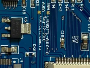
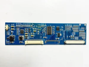
PCB stands for Printed Circuit Board, the abbreviated term for printed circuit boards.
Typically, engineers form conductive patterns on insulating materials according to predetermined designs—either as printed circuits, printed components, or a combination of both—and refer to them as printed circuits.
Conductive patterns on insulating substrates that connect components electrically are called printed circuits.
Thus, manufacturers call the finished board, which contains either a printed circuit or printed wiring, a printed circuit board, also known as a PCB.
PCBs are indispensable in nearly every electronic device we encounter—from small items like electronic watches, calculators, and general-purpose computers to large systems such as computers, communication electronics, and military weaponry.
Any device incorporating integrated circuits or other electronic components relies on PCBs for electrical interconnection.

Classification
The electroplating processes for printed circuit boards can be broadly categorized as follows:
1. Acidic bright copper plating
2. Nickel/gold plating
3. Tin plating
Process Flow
Acid Immersion → Full-Panel Copper Plating → Pattern Transfer → Acid Degreasing → Two-Stage Countercurrent Rinsing → Micro-Etching → Second Stage → Acid Immersion → Tin Plating → Two-Stage Countercurrent Rinsing

Counter-current rinsing → Acid immersion → Pattern copper plating → Two-stage counter-current rinsing → Nickel plating → Two-stage water rinsing → Citric acid immersion → Gold plating → Recovery → 2-3 stages of pure water rinsing → Drying

1. Acid Pickling
① Function and Purpose: Removes surface oxides and activates the board surface.
Typically maintained at 5% concentration, though some systems keep it around 10% to prevent moisture contamination from destabilizing sulfuric acid levels in the bath.
② Avoid prolonged acid immersion to prevent plate oxidation.
Replace the acid solution promptly when it becomes cloudy or exhibits excessively high copper content after prolonged use to prevent contamination of the copper plating bath and plate surfaces.
③ Use C.P. grade sulfuric acid for this process.
2. Full-Panel Copper Plating
Full-Panel Copper Plating (Primary Copper Plating / Panel Plating)
(1). Function and Purpose
Full-panel copper plating protects the newly deposited thin layer of chemical copper, preventing oxidation and subsequent acid etching.
Electroplating builds up the layer to a specified thickness.
(2). Key Process Parameters
The bath solution primarily contains copper sulfate and sulfuric acid, using a high-acid, low-copper formulation to ensure uniform thickness across the panel surface and enhance penetration into deep holes and small apertures.
Sulfuric acid concentration: 180–240 g/L
Copper sulfate content: ~75 g/L
Trace chloride ions act as auxiliary brighteners, enhancing luster with copper brighteners
Copper brightener dosage: 3–5 mL/L initially; replenishment based on the thousand ampere-hour (KAH) method or actual production results
Full-panel plating current: 2 A/dm² × panel length (dm) × panel width (dm) × 2
Bath temperature: typically 22°C, not exceeding 32°C; install cooling in hot weather
(3). Process Maintenance
Replenish copper brightener daily at 100–150 mL/KAH
Check filter pump operation and look for air leaks
Clean cathode conductive rods every 2–3 hours
Analyze copper sulfate and sulfuric acid once per week, chloride ions twice per week
Adjust brightener concentration via Hall cell tests and replenish raw materials promptly
Clean anode rods and electrical terminals weekly
Replenish anode copper balls in titanium baskets
Perform low-current electrolysis (0.2–0.5 ASD) for 6–8 hours
Inspect anode baskets monthly and replace if damaged
Remove anode sludge from baskets and clean thoroughly
Perform continuous carbon core filtration for 6–8 hours during low-current electrolysis
Conduct major treatment with activated carbon powder approximately every six months
Replace filter pump cartridges biweekly
(4). Major Treatment Procedure
① Remove anodes, empty contents, clean surface film, and store in copper anode packaging drums.
② Roughen copper corners with micro-etchant until uniform pink; rinse and store in acid tank.
③ Immerse anode titanium basket in 10% alkaline solution for 6–8 hours; rinse, soak in 5% dilute sulfuric acid, rinse again.
④ Transfer bath solution to standby tank; add 1–3 mL/L of 30% hydrogen peroxide and heat to ~65°C while agitating for 2–4 hours.
⑤ Dissolve activated carbon powder slowly (3–5 g/L), reactivate agitation, and maintain for 2–4 hours.
⑥ Let carbon settle, filter bath through 10 μm PP filter into a clean tank.
⑦ Hang anodes and electrolytic plates; perform low-current electrolysis (0.2–0.5 ASD) for 6–8 hours.
⑧ Adjust sulfuric acid, copper sulfate, and chloride ion concentrations; supplement brighteners based on Hall cell tests.
⑨ Form uniform black phosphoric film at 1–1.5 ASD for 1–2 hours; test plating quality.
(5). Chemical Handling Notes
Anode copper balls contain 0.3–0.6% phosphorus to reduce dissolution and minimize copper powder.
Perform low-current electrolysis after large chemical additions.
Add sulfuric acid slowly in batches to prevent temperature spikes, accelerated brightener decomposition, and bath contamination.
Measure chloride ions carefully (30–90 ppm); 1 mL HCl contains ~385 ppm chloride.
Chemical Addition Formulas
Copper sulfate (kg) = (75 – X) × tank volume (L) / 1000 Sulfuric acid (L) = (10% – X) g/L × tank volume (L) or (180 – X) g/L × tank volume (L) / 1840
Hydrochloric acid (mL) = (60 – X) ppm × tank volume (L) / 385
3. Acid Degreasing
① Purpose and Function: Removes oxides from the copper surface of the circuit, along with residual ink film and adhesive, ensuring adhesion between the base copper and the patterned electroplated copper or nickel.
② Note: Why use an acidic degreaser here instead of an alkaline one, despite alkaline degreasers being more effective?
Primarily because patterned ink is incompatible with alkalis, which would damage circuit patterns.
Thus, only acidic degreasers can be used before pattern plating.
③ During production, only the degreaser concentration and time need to be controlled.
The degreaser concentration should be around 10%, and the time should be maintained at 6 minutes. Slightly longer times will not cause adverse effects.
The bath solution replacement rate is 15 square meters per liter of working solution, and the replenishment rate is 0.5–0.8 liters per 100 square meters.
4. Micro-etching
① Purpose and Function: Clean and roughen the copper surface of the circuit lines to ensure adhesion between the plated copper pattern and the primary copper layer.
② Sodium persulfate is commonly used as the micro-etchant. It provides stable and uniform roughening rates with good water-washability.
Concentration is typically maintained at approximately 60 g/L, with processing time controlled around 20 seconds.
Chemical addition rate is 3-4 kg per 100 m². Copper content should be kept below 20 g/L. Other maintenance and tank replacement procedures follow those for electroplating copper micro-etching.
5. Acid Pickling
① Function and Purpose:
Removes surface oxides and activates the board surface. Typically maintained at 5% concentration, though some systems keep it around 10% to prevent moisture introduction from destabilizing sulfuric acid levels in the bath.
② Avoid prolonged acid immersion to prevent plate oxidation.
Replace the acid solution promptly when it becomes cloudy or exhibits excessively high copper content after prolonged use to prevent contamination of the copper plating bath and plate surfaces.
③ Use C.P. grade sulfuric acid for this process.
Common Data in PCB Electroplating
Electrolytic Equivalents of Selected Elements
Element Name Atomic Weight Chemical Equivalent Valence Electrolytic Equivalent (g/AH)
- Silver Ag 107.868 107.868 14.0247
- Gold Au 196.9665 196.9665 17.357
- Copper Cu 63.5463 1.7732 1.185
- Nickel Ni 58.7029 3.8654
- Tin Sn 118.695a 9.3452 2.1422
Standard Electrode Potential of Some Metals in Aqueous Solution
- Ag/Ag⁺: 0.799
- Cu/Cu²⁺: 0.345
- Ni/Ni²⁺: -0.250
- Sn/Sn²⁺: -0.140
- Au/Au⁺: 1.70
Current Efficiency of Certain Electroplating Solutions
- Nickel Plating: 95–98%
- Sulfate Copper Plating: 95–100%
- Lead-Tin Alloy Plating: 100%
- Palladium Plating: 90–95%
- Cyanide Gold Plating: 60–80%
PH Values for Precipitation of Metal Hydroxides
Hydroxide begins to precipitate
Initial ion concentration:
- Residual ion concentration <10-5mol/L
- Stannous hydroxide 0.05 mol/L11315
- Stannous hydroxide0.92.14.71013.5
- Iron(III) hydroxide 1.5 2.3 4.1 14
- Silver oxide 6.2 8.2 11.2 12.7
- Ferrous hydroxide 6.5 7.5 9.7 13.5
- Cobalt hydroxide 6.6 7.6 9.2 14.1
- Nickel hydroxide 6.7 7.7 10.4
Quality of 1μm Plating
- Copper: 0.089 g/dm²
- Gold: 0.194 g/dm²
- Silver: 0.105 g/dm²
- Tin: 0.073 g/dm²
- Nickel: 0.089 g/dm²
Conclusion
PCB electroplating is a highly controlled and chemistry-intensive process that directly impacts circuit reliability, conductivity, and product lifespan.
Through careful management of each step—such as acid pickling, full-panel copper plating, degreasing, and micro-etching—manufacturers can ensure strong adhesion, uniform thickness, and consistent electrical performance.
By combining standardized process control, precise chemical replenishment, and data-driven maintenance practices, PCB manufacturers can achieve stable production quality, reduce defects, and meet the increasingly demanding requirements of advanced electronic applications.