
PCB routing is a critical stage in circuit board design that directly impacts product performance, signal integrity, and manufacturing yield.
As modern electronic devices become increasingly compact and high-speed, designers face growing challenges in balancing signal quality, noise suppression, and cost efficiency.
This guide explores essential PCB routing techniques, from ground sharing strategies in mixed-signal circuits to advanced via design optimization for high-speed applications.
Whether you’re a beginner or an experienced engineer, mastering these principles will help you achieve more reliable, efficient, and cost-effective PCB layouts.
Ground Sharing in Digital and Analog Circuits
Today, many PCBs are no longer single-function circuits (either digital or analog), but rather consist of a mix of digital and analog circuits.
Therefore, when routing traces, it is necessary to consider the issue of mutual interference between them, particularly noise interference on the ground lines.
Digital circuits operate at high frequencies, while analog circuits are highly sensitive.
For signal lines, designers should route high-frequency signal lines as far away as possible from sensitive analog components.
As for ground lines, the entire PCB has only one connection point to the outside world;
Therefore, designers must resolve the shared ground issue between digital and analog circuits inside the PCB.
On the board itself, designers keep digital ground and analog ground separated without interconnection.
The only connection point lies at interfaces where the PCB links to external equipment, such as connectors.
There is a single short-circuit connection between the digital ground and the analog ground—please note that there is only one connection point.
Some PCBs do not share a common ground, which is determined by the system design.
Routing Signal Lines on Power (Ground) Layers
When routing on multilayer printed circuit boards, since there is little unused space left on the signal layers, adding more layers would result in waste and increase the production workload, thereby raising costs.
To resolve this issue, consider routing on power (ground) layers.
Designers should prioritize the power layer first, then use the ground layer, so they can maintain the integrity of the ground layer.
Handling of Component Leads in Large-Area Conductors
Designers usually connect component leads to conductors in large-area grounding systems.
The handling of these leads requires comprehensive consideration.
From an electrical performance perspective, designers prefer fully connecting component lead pads to the copper surface.
However, this approach poses certain risks to the soldering and assembly process, such as:
① Soldering requires a high-power heater. ② It can easily lead to cold solder joints.
Therefore, to balance electrical performance and manufacturing requirements, a cross-shaped pad is used, known as a “heat shield” or colloquially as a “thermal pad.”
This significantly reduces the likelihood of cold solder joints caused by heat dissipation due to excessive cross-sectional area during soldering.
The same treatment applies to component leads on the power (ground) layers of multilayer boards.
Role of the Network System in Routing
In many CAD systems, routing is determined by the network system.
If the grid is too dense, although the number of routing paths increases, the step size becomes too small, resulting in an excessive amount of data in the drawing.
This inevitably places higher demands on device storage capacity and also significantly impacts the processing speed of the host computer and other electronic devices.
Furthermore, some paths are invalid, such as those occupied by component lead pads, mounting holes, or stenciling holes.
Conversely, if the grid is too sparse, the limited number of routing paths greatly affects the routing success rate.
Therefore, a reasonable grid system is necessary to support the routing process.
The standard distance between the legs of a component is 0.1 inch (2.54 mm), so the basis of the grid system is generally set to 0.1 inch (2.54 mm) or an integer multiple of 0.1 inch, such as 0.05 inch, 0.025 inch, or 0.02 inch.
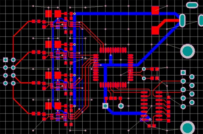
Handling Power and Ground Lines
Even if the routing of the entire PCB is completed properly, interference may still arise.
This interference stems from insufficient planning for power and ground traces.
It can deteriorate the overall performance of the product. In certain situations, it may even lower the production yield.
Therefore, the routing of power and ground lines must be taken seriously to minimize noise interference generated by them and ensure product quality.
Every engineer involved in electronic product design understands the causes of noise between ground and power lines;
Here, we will focus solely on methods to reduce or suppress this noise:
Designers know they should add decoupling capacitors between power traces and ground traces.
Make the power and ground traces as wide as possible, ensuring that the ground trace is wider than the power trace.
The relative widths should be: ground trace > power trace > signal trace.
Typically, signal traces are 0.2–0.3 mm wide, with fine traces as narrow as 0.05–0.07 mm, while power traces are 1.2–2.5 mm wide.
For digital circuit PCBs, designers can use wide ground traces to form a loop and build an effective ground plane.
Do not adopt this method for analog circuits. Designers can use a large copper area as the ground plane.
They should connect all vacant areas on the printed circuit board to ground to act as ground traces.
Alternatively, a multilayer board can be used, with the power and ground traces each occupying a separate layer.
Design Rule Check (DRC)
After designers finish routing the design, they must conduct thorough checks to make sure the layout complies with their defined design rules.
It is also necessary to verify that these rules meet the requirements of the printed circuit board manufacturing process.
Generally, the following aspects are checked: whether the distances between traces, between traces and component pads, between traces and vias, between component pads and vias, and between vias are appropriate and meet production requirements.
Are the widths of power and ground traces appropriate, and are power and ground traces tightly coupled (low signal impedance)?
Are there any areas on the PCB where ground traces can be widened?
Have measures been taken for critical signal lines, such as keeping them short, adding shielding traces, and clearly separating input and output lines?
Do the analog and digital circuit sections have their own independent ground planes?
Could graphics added to the PCB (such as icons and annotations) cause signal short circuits?
Modify any suboptimal trace routing. Are process lines included on the PCB?
Does the solder mask meet production requirements? Are the solder mask dimensions appropriate?
Are character markings positioned over component pads to avoid affecting assembly quality?
In multilayer boards, are the outer edges of the power and ground planes recessed?
If copper foil from the power or ground planes extends beyond the board edges, it can easily cause short circuits.
Via Design
Vias: A Critical Component and Major Cost Factor in Multilayer PCBs
Vias are one of the key components of multilayer PCBs, and the cost of drilling typically accounts for 30% to 40% of the total PCB manufacturing cost.
Simply put, designers call every hole on a PCB a via. Designers separate vias into two groups based on their functions:
Those used for electrical connections between layers, and those used for securing or positioning components.
From a manufacturing process perspective, vias are generally classified into three types: blind vias, buried vias, and through vias.
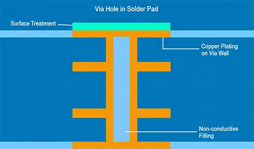
Three Types of Vias: Blind, Buried, and Through Vias
Blind vias are located on the top and bottom surfaces of a printed circuit board (PCB) and have a certain depth;
They are used to connect surface-level traces to the underlying internal layers.
The depth of these vias typically does not exceed a certain ratio (of the via diameter).
Buried vias refer to connection holes located within the internal layers of a PCB;
They do not extend to the board’s surface.
Designers embed these two types of vias within the PCB’s inner layers.
They are manufactured through the through-hole drilling process before board lamination.
Multiple internal layers may be stacked together in the course of via fabrication.
Designers call the third type a through-hole. It runs through the entire PCB.
Designers can use through-holes for internal interconnections or as mounting and positioning holes for components.
Since through-holes are easier to manufacture and less expensive, they are used in the vast majority of printed circuit boards, rather than the other two types of vias.
Unless otherwise specified, the term “via” as used below refers to through-holes.
Via Structure and Size: Balancing Routing Space and Manufacturing Limits
From a design perspective, a via consists primarily of two parts: the central drill hole and the pad area surrounding the drill hole.
The dimensions of these two parts determine the size of the via.
Obviously, when designing high-speed, high-density PCBs, designers always prefer vias to be as small as possible, as this leaves more space on the board for routing.
Furthermore, the smaller the via, the lower its parasitic capacitance, making it more suitable for high-speed circuits.
However, reducing the hole size also increases costs, and the size of a via cannot be reduced indefinitely;
It is limited by manufacturing processes such as drilling and plating: the smaller the hole, the longer it takes to drill, and the more likely it is to deviate from the center position;
Furthermore, if the hole depth exceeds six times the drill diameter, manufacturers cannot guarantee uniform copper plating on the hole walls.
For example, a standard 6-layer PCB normally has a thickness (via depth) of around 50 mils.
Therefore, PCB manufacturers can only supply drill diameters up to 8 mils.
Parasitic Capacitance: How Vias Slow Down Signal Rise Time
Parasitic Capacitance of Via Holes Via holes inherently have parasitic capacitance to ground.
If designers define D2 as the isolation hole diameter of a via on the ground plane, D1 as the via pad diameter, T as the PCB thickness, and ε as the dielectric constant of the substrate material, they can calculate the via’s parasitic capacitance with this approximate formula:
C = 1.41εTD1/(D2 − D1) The main effect of a via’s parasitic capacitance on a circuit is to prolong the signal rise time and reduce the circuit’s speed.
The parasitic capacitance of a via exerts a notable influence on circuit performance.
It extends the signal rise time and lowers the operating speed of the circuit.
Take a practical case for illustration. The PCB thickness is 50 mils.
The selected via has a drill hole inner diameter of 10 mils and a pad diameter of 20 mils.
The clearance between the via pad and the ground plane equals 32 mils. Substitute these parameters into the formula for estimation: C = 1.41 × 4.4 × 0.050 × 0.020 / (0.032 – 0.020) = 0.517 pF.
The change in rise time caused by this capacitance is: T10–90 = 2.2C(Z0/2) = 2.2 × 0.517 × (55/2) = 31.28 ps.
These calculation results illustrate an important point.
The parasitic capacitance of a single via has limited impact on slowing down signal rise time.
However, designers need to treat this factor cautiously.
This is especially true when a signal trace uses multiple vias to transition between different PCB layers.
Parasitic Inductance and High-Speed Via Design Optimization
1. Parasitic Inductance: Why It Outweighs Capacitance in High-Speed Design
Parasitic Inductance of Via Holes: Just as via holes have parasitic capacitance, they also have parasitic inductance.
In the design of high-speed digital circuits, the adverse effects caused by the parasitic inductance of via holes often outweigh those of parasitic capacitance.
The parasitic series inductance of a via hole weakens the contribution of bypass capacitors, thereby reducing the filtering effectiveness of the entire power supply system.
2. Inductance Calculation: Formula, Example, and Equivalent Impedance
We can use the following formula to roughly calculate the approximate parasitic inductance of a via: L = 5.08h [ln(4h/d) + 1], where L is the inductance of the via, h is the length of the via, and d is the diameter of the center drill hole.
As can be seen from the equation, the diameter of the via has a relatively small effect on inductance; rather, it is the length of the via that primarily affects inductance.
Using the example above, we can calculate the inductance of the via as: L = 5.08 × 0.050 [ln(4 × 0.050 / 0.010) + 1] = 1.015 nH.
If the signal’s rise time is 1 ns, its equivalent impedance is: XL = πL/T × 10⁻⁹ = 3.19 Ω.
Designers cannot ignore this impedance when high-frequency currents flow through the circuit.
It is particularly important to note that when a bypass capacitor connects the power plane to the ground plane, it must pass through two vias, which causes the parasitic inductance of the vias to increase exponentially.
3. Five Practical Guidelines for Minimizing Via Parasitic Effects
Based on the above analysis of via parasitic characteristics, we can see that in high-speed PCB design, vias that appear simple can often have significant negative effects on circuit design.
To minimize the adverse effects brought by via parasitic characteristics, designers should follow the practices below as much as possible throughout the design process.
1). Select a reasonable via size, taking both cost and signal quality into consideration.
For example, in the design of 6- to 10-layer memory module PCBs, 10/20 mil (drill/pad) vias are preferable.
For some compact, high-density circuit boards, designers can also consider using 8/18 mil vias.
Given current technological limitations, it is difficult to use vias smaller than this.
For power or ground vias, designers can consider adopting larger sizes to lower impedance.
2). As can be deduced from the two formulas discussed above, using a thinner PCB helps reduce both types of parasitic parameters in vias.
3). Signal traces on the PCB should change layers as little as possible; in other words, avoid using unnecessary vias.
4). Power and ground pins should have vias placed as close as possible;
The shorter the traces between the vias and the pins, the better, as longer traces increase inductance.
At the same time, power and ground traces should be as wide as possible to reduce impedance.
5). Place some ground vias near the vias where signal traces change layers to provide a nearby return path for the signals.
You can even place a large number of extra ground vias on the PCB. Of course, flexibility is essential during the design process.
The via models discussed earlier assume that pads are present on every layer;
However, in some cases, we can reduce or even eliminate pads on certain layers.
This is particularly important when via density is very high, as it may create a gap in the copper plane that interrupts the return path.
To resolve this issue, in addition to repositioning the vias, we can also consider reducing the size of the via pads on that copper layer.

