PCB soldering quality is not determined by a single process step, but by the coordinated control of design, materials, equipment, and human operation throughout the entire manufacturing flow.
From PCB layout and board fabrication to component placement and reflow soldering, each stage introduces variables that can directly affect solder joint reliability and assembly yield.
This article systematically analyzes the key factors that influence PCB soldering quality.
It places particular emphasis on design-related considerations, which often determine soldering success or failure even before production begins.
Factors Affecting PCB Soldering Quality
From PCB design to the completion of all component soldering, achieving a high-quality circuit board requires control across multiple stages involving PCB engineers, soldering processes, and soldering technicians.
The key factors influencing PCB soldering include PCB layout and circuit board quality. Component quality and the oxidation level of the component also play a significant role.
Additionally, solder paste quality and the accuracy of solder paste printing affect soldering outcomes.
The precision of placement machine programming and the assembly quality of the placement machine are critical.
Finally, the temperature profiles of the reflow oven significantly impact soldering quality.
The PCB layout itself represents an insurmountable challenge for soldering factories.
Circuit designers rarely solder boards themselves, limiting their hands-on soldering experience.
Conversely, factory workers lack design expertise, focusing solely on production targets without the mindset or analytical skills to diagnose soldering defects.
These two specialized roles operate in silos, making seamless integration challenging.
Recommendations for PCB Design
Below are some suggestions to avoid poor design practices that may compromise soldering quality.
Regarding Positioning Holes
Four holes (minimum diameter 2.5mm) must be reserved at the four corners of the PCB board for positioning the circuit board during solder paste printing.
The centers of the holes on the X-axis or Y-axis must be aligned on the same axis, as shown below:

Regarding Mark Points
Mark points must be marked on the PCB board for placement machine positioning.
Specific location: Diagonally opposite corners of the board. These can be circular or square pads, and must not be mixed with pads for other components.
If components are present on both sides, mark points must be added to both sides.
Consider adding mark points to panel layouts as well.
When designing PCBs, Note the Following
a. Marker point shapes should follow the reference pattern below, being either vertically symmetrical or horizontally symmetrical.

b. The size of A is 2.0mm.
c. Within 2.0mm of the outer edge of the Mark point, there should be no shapes or color variations that could cause misidentification (e.g., pads, solder paste).
d. The color of the Mark point must contrast distinctly with the surrounding PCB surface.
e. To ensure recognition accuracy, the Mark point surface shall be plated with copper or tin to prevent reflection.
Markers consisting solely of lines cannot be recognized by the light spot.
As shown below:

Regarding the 5mm Border
When designing PCBs, leave a border of at least 3mm along the longer side for conveying the board during SMT placement.
Components must not be placed within this area, as the placement machine cannot mount components here.
As shown in the figure:

For double-sided ornamental circuit boards, consider issues such as component displacement and pad displacement during secondary reflow soldering.

It is recommended that no surface-mount components be placed within 5mm of the edge along the longer side of the chip-side.
If PCB space constraints necessitate placement, components may be placed along the longer edge’s process edge.
Do not Drill Vias Directly on Pads
Drilling vias on pads allows solder paste to flow into the vias during reflow soldering, causing solder deficiency on the component pads and resulting in cold solder joints, as shown in the figure below.

Polarity Markings for Diodes and Tantalum Capacitors
Polarity markings for diodes and tantalum capacitors comply with industry standards to prevent workers from soldering them in the wrong direction based on experience.
As shown in the figure:

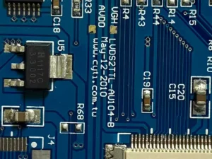
Regarding Silk Screen and Markings
Please conceal part numbers, especially on high-density circuit boards. Otherwise, the cluttered appearance hinders locating soldering positions. As shown below:

Do not label only the model number without indicating the grade. As shown in the figure below, this prevents programming of the placement machine.

The font size of silk-screened characters should not be too small, and characters should be positioned away from vias to prevent misreading.

Regarding IC Pad Length Extension
For ICs in packages such as SOP, PLCC, and QFP, the optimal pad length on the PCB should be 1.5 times the IC pin length.
This facilitates manual soldering with a soldering iron, ensuring the chip pins, PCB pads, and solder melt into a single, integrated joint. As shown in the figure:

Regarding IC Pad Width
When designing PCBs for ICs in packages such as SOP, PLCC, and QFP, pay attention to pad width.
The width of pad a on the PCB should equal the IC pin width (the Nom. value in the datasheet).
It is not recommended to widen it. Ensure sufficient spacing b between pads to prevent bridging. As shown in the figure:

Do not Rotate Components to Arbitrary Angles
Since the placement machine cannot rotate to arbitrary angles, it can only rotate at 90°, 180°, 270°, or 360°.
As shown in Figure B below, rotating by 1° will cause the component leads to be misaligned by 1° relative to the pads on the circuit board after placement, thereby affecting soldering quality.

Considerations for Shorting Adjacent Pins
The shorting method shown in Figure a is difficult for workers to identify and results in an unattractive appearance after soldering.
If shorting is implemented as shown in Figures b and c during the design phase and the solder mask is applied, the soldering outcome will be significantly different.
As long as each pin remains isolated, the chip will not experience short circuits and will maintain an aesthetically pleasing appearance.

Regarding the Central Pad Under the Chip
For chips with a raised center pad, it is recommended to reduce the size of the central pad to increase its distance from surrounding pads, thereby minimizing the risk of short circuits. As shown below:

Do not Place Two Thicker Components in Close Proximity to Each Other
As shown in the figure below, this layout will cause the pick-and-place machine to collide with the previously placed component when placing the second component.
The machine will detect a hazard and automatically shut down.

About BGAs
Due to the unique nature of BGA packaging, where all pads are located beneath the chip, soldering results are not visible externally.
For easier rework, it is recommended to drill two 30mil positioning holes on the PCB to facilitate stencil alignment during rework.
Note: The size of the alignment holes should not be too large or too small.
They should be snug enough that the pins do not fall out or wobble when inserted, but not so tight that they cannot be inserted. Otherwise, inaccurate positioning may occur. See the figure below:

Regarding PCB Board Colors
It is recommended not to use red.
Red circuit boards appear white under the red light source of the pick-and-place machine’s camera, making programming impossible and hindering the pick-and-place machine’s soldering process.
Regarding Small Components Under Large Components
Some prefer to arrange small components beneath larger ones on the same layer.
For example, resistors are placed beneath a seven-segment display, as shown below:

This layout makes repairs difficult, as the LED display must be disassembled first, potentially causing damage to the display.
It is recommended to relocate the resistors beneath the LED display to the bottom side, as shown in the figure below:

Regarding the Impact of Copper Cladding Connections on Solder Melting
Since copper cladding absorbs significant heat, it hinders the solder from melting sufficiently, leading to cold solder joints. As shown in the figure:

In Figure a, the device pads are directly connected to the copper cladding.
In Figure b, although the 50-pin connector is not directly connected to the copper cladding, the two middle layers of the four-layer board are large copper areas.
Therefore, both Figure a and Figure b will cause the solder paste to fail to fully melt due to the copper cladding absorbing a large amount of heat.
The body of the 50-pin connector in Figure b is made of heat-sensitive plastic. If the temperature is set too high, the connector body may melt or deform.
If the temperature is set too low, the copper cladding absorbs excessive heat, preventing the solder paste from melting sufficiently.
Therefore, it is recommended to isolate the pads from the large copper cladding areas. As shown in the figure:

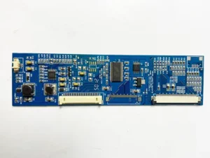
Recommendations for Panel Joining and Processing Techniques


Summary
Nowadays, an increasing number of engineers can use software to draw diagrams, design, and route PCBs. Once the design is complete, it can significantly improve soldering efficiency.
The author believes that the above factors require particular attention.