Printed circuit boards (PCBs) provide interconnections for electronic components and parts, forming modules or finished products with specific functions.
PCB types and manufacturing methods vary in materials, layers, and production processes, enabling adaptation to different electronic products and specialized requirements.
Removing gold-plated leads from PCB edge connectors via etching effectively enhances product performance and stability.
However, this method involves a lengthy production process, increased quality risks during processing, and higher manufacturing costs.
For removing gold-plated leads from graphics card edge connectors, a charge-coupled device (CCD) to position the process.
Gold plating is applied to the lead between two pins. After plating, CCD back drilling severs the gold-plated lead at a controlled depth of 0.1–0.2 mm.
The drill hole diameter aligns tangentially with the connector pitch, maintained within a tolerance of ±0.05 mm.
The protrusions on the pin edges are controlled within ±0.05 mm (to prevent drill damage and lead residue).
This process streamlines steps, reduces labor hours, and lowers costs.
The CCD back-drilling lead method establishes a feasible technical solution covering engineering design, process flow, key process control points, comparison between etched leads and CCD back-drilled lead products, and CCD back-drilling process capability data verification.
PCB Gold-Plated Lead Requirements
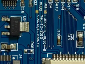
For PCIE 5.0 graphics card designs, at the board edge connector end position, residual gold-plated leads from PCB manufacturing are unacceptable as shown in Figure 1.
After gold plating, remove the leads using a reverse etching process.

Graphics Card Board Edge Connector Position Removal Method for Electroplated Leads
Etching Lead Process
Material Cutting → Inner Layer → Laminating → Mechanical Drilling → Plasma Deburring, Electroless Copper Plating → Board Electroplating → Outer Layer → Solder Mask → Text Printing → Solder Mask Printing → Oil Removal → Sandblasting → Gold Plating → Film Removal → Sandblasting (2) → Solder mask printing and organic solderability preservation (OSP) (2) → Outer layer (2) → Film removal (2) → Outer layer inspection (automatic optical inspection, AOI) (2) → Forming → Testing → Final quality control (FQC) → Anti-oxidation coating (organic solderability preservation, OSP) → Packaging.
CCD Back Drilling Lead Process
Material Cutting → Inner Layer Assembly → Laminating → Mechanical Drilling → Plasma Resin Removal & Electroless Copper Plating → Board Electroplating → Outer Layer Assembly → Solder Mask Application → Text Printing → Gold Plating → Mechanical Drilling (2) → Mechanical Drilling (3) → Forming → Testing → FQC → OSP → Packaging.
Note: Etched leads involve 6 additional processes compared to CCD back drilling, resulting in a longer production cycle and extended lead times. CCD back drilling enhances production efficiency, shortens delivery times, and eliminates potential quality risks associated with etched leads.
Differences Between Etched Leads and CCD Back-Drilled Leads
The impact of etched leads and back-drilled leads on PCB quality is illustrated in Figure 2.
Etched leads expose copper within ±0.1 mm at the tip, while back-drilled leads leave ±0.05 mm of residue.
Due to the additional post-processing steps involved, etched leads may also suffer from incomplete film removal, pad (plate and disc, PAD) contamination by chemical solutions, and ink peeling/color variation issues.

Full Process of CCD Back Drilling Lead Technology
Engineering Graphic Design Plan
(1) The PCIE 5.0 graphics card pins transition from etched leads to back drilling. Dimensions are set as shown in Figure 3.

(2) For CCD back drilling, initial positioning holes are drilled at the four corners of the PNL edge at 3.175 mm.
Production alignment is achieved by scanning one optical point at each corner within the panel, as illustrated in Figure 4.

CCD Back Drilling Lead Wire
Key process control points for CCD back drilling lead wires are shown in Table 1.
Each step must be performed according to requirements to ensure the manufactured products meet expected specifications.
| Department | Process | Key Process Control Points |
|---|---|---|
| Engineering Department | Production Manufacturing Instruction (MI) | After design completion, notify production, process, project, and quality responsible departments. Add one set of 3.175 mm tooling holes (four holes) for first back-drill positioning and avoid interference with original 3.175 mm targets. Original targets used for outer-layer alignment and drill guide positioning. |
| Engineering Department | Computer Aided Manufacturing (CAM) | Prepare two sets of production programs (CCD program, four-hole machine program). Generate drill guide strip program according to outer-layer scaling factors. |
| Drilling | First Drill | Confirm addition of one set of 3.175 mm tooling holes (four holes) and control of 3.175 mm drill bit. |
| Outer Layer Circuit | Outer Layer | PED value controlled at ±50 μm. Panel boards separately according to different scaling factors. |
| Gold Plating | Gold Plating | Panel boards separately according to different scaling factors to reduce separation during CCD back-drill guide processing. |
| Counterbore / Step Hole | Drill Counterbore and Remove Guide Strip | Confirm positioning method using outer-layer optical target alignment. Follow engineering-provided outer-layer scaling factors for gold-plated guide strip drilling. First article cross-section and secondary dimensional data; in-process secondary sampling confirmation. |
Process Capability Assessment
Process Capability of Lead Residue Size Between Pins for Back Drilling Different Hole Diameters
(1) Hole diameter 0.5 mm, lead residue ±0.05 mm.
Due to the combined effects of equipment precision and cutting tools, the measured mean protrusion of lead residue was 0.014 mm, while the measured mean indentation at pin drilling was 0.011 mm, both within the lead residue tolerance range (see Figure 5).
Process capability was verified using 30 sets of measured data.
The Cpkfor lead residue was 2.29, while the Cpk for drilling to pin was 1.77.
The overall Cpk process capability index was 1.33, as shown in Figure 6.


(2) Hole diameter: 0.4 mm; lead residue tolerance: ±0.05 mm.
Following the same measurement and process capability analysis, the 0.4 mm hole diameter position was influenced by both equipment precision and cutting tools.
The measured mean protrusion for lead residue was 0.016 mm, while the measured mean indentation for drilling into pins was 0.011 mm.
Both values fell within the lead residue tolerance range, meeting the qualification criteria.
Process capability verification was conducted using 30 data sets each.
The Cpkfor lead residue was 1.63, and the Cpk for drilling to pin was 2.03. The overall Cpk process capability index was 1.33.
Process Capability of Back Drill Hole Diameter
The measured mean for 0.5 mm back drill holes was 0.51 mm, and for 0.4 mm back drill holes it was 0.41 mm, both within the ±0.05 mm tolerance range, as shown in Figure 7.
Process capability was verified using 30 data sets each.
The Cpk for the 0.5 mm hole diameter was 1.67, and for the 0.4 mm hole diameter, it was 1.54.
The overall Cpk process capability index was 1.33, as shown in Figure 8.


Process Capability of Back Drilling Depth (Distance from Board Plane to Lowest Point of Hole)
For back drilling depths of 0.5 mm and 0.4 mm hole diameters (distance from board plane to lowest point of hole), the upper control limit for 0.5 mm back drilling depth is 0.125 mm, and for 0.4 mm back drilling depth, it is 0.100 mm.
(1) The mean depth for 0.5 mm back drilling is 0.08 mm, deemed acceptable as shown in Figure 7(a).
Process capability was verified using 30 data sets per measurement.
The Cpkfor the 0.125 mm upper limit is 1.8, with a Cpk process capability index of 1.33.
The 0.125 mm upper limit Cpk is acceptable. At the 0.100 mm upper limit, Cpk was 0.77, with a process capability index of 1.33.
The Cpk at the 0.100 mm upper limit was non-conforming.
The mean was 0.08 mm, which did not exceed the upper limit of 0.1 mm, thus deemed acceptable, as shown in Figure 9.

(2) The average depth of the 0.4 mm back drill hole was 0.067 mm, as shown in Figure 7(b).
Process capability verification was conducted using 30 sets of data.
The Cpkfor the 0.125 mm upper limit was 4.38, while the Cpk for the 0.100 mm upper limit was 2.5.
The overall Cpk process capability index was 1.33. CCD back-drilled lead products underwent process capability data verification, with all test results meeting specifications.
Conclusion
This paper introduces an alternative method to etching lines: utilizing CCD back-drilled leads, drawing gold-plated leads between two pins, and after plating completion, severing the gold-plated leads via CCD back-drilled holes.
The drilling depth is controlled between 0.1 and 0.2 mm, with hole diameters tangential to the pin pitch. with hole diameter tolerance controlled at ±0.05 mm and lead residue at pin edges controlled at ±0.05 mm.
This method reduces the production process by 6 steps, enhancing efficiency and lowering manufacturing costs. Part Number EQ
Switching from etched leads to CCD back-drilled leads. New samples and new customer orders confirm the adoption of CCD back-drilled lead production.
Utilizing the CCD back-drilled leads designed herein achieves a breakthrough in optimizing the manufacturing process for graphics card etched lead variants from a design perspective.