Numerous empirical formulas, correlation tables, and software tools regarding PCB trace width and current are available online.
The following summarizes eight different formulas, tables, and calculation methods for the relationship between current and trace width.
Although these vary slightly (while generally similar), designers can select an appropriate trace width in actual PCB board design by comprehensively considering the board size and current requirements.
PCB Current and Trace Width
Calculating PCB current carrying capacity has long lacked authoritative technical methods or formulas.
Experienced CAD engineers can make relatively accurate judgments based on personal expertise. However, for CAD novices, this presents a significant challenge.
PCB current carrying capacity depends on the following factors: trace width, trace thickness (copper foil thickness), and allowable temperature rise.
Wider PCB traces have greater current carrying capacity. Assuming identical conditions, if a 10MIL trace can handle 1A, can a 50MIL trace handle 5A? The answer is clearly no.
Refer to the following data from an internationally recognized authority: Trace width units: Inch (1 inch = 2.54 cm = 25.4 mm); Data source: MIL-STD-275 Printed Wiring for Electronic Equipment.
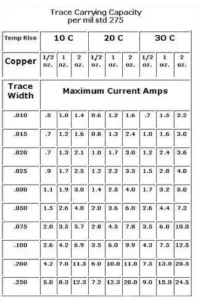
Relationship Between PCB Copper Thickness, Trace Width, and Current
Before exploring the relationship between PCB copper thickness, trace width, and current, let’s first understand the conversion between ounces, inches, and millimeters for PCB copper thickness: “In many datasheets, PCB copper thickness is often specified in ounces.
Its conversion relationships with inches and millimeters are as follows:
1 oz = 0.0014 inches = 0.0356 millimeters (mm);
2 oz = 0.0028 inches = 0.0712 millimeters (mm);
Ounces measure weight. We can convert them to millimeters because PCB copper thickness is defined in ounces per square inch.
The table below shows the relationship between copper thickness, line width, and current in PCB design:
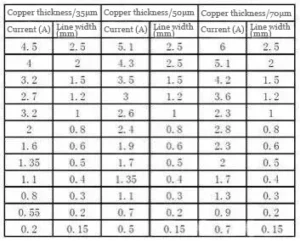
You can also use an empirical formula for the calculation: 0.15 × line width (W) = A.
All data above represent the current carrying capacity of the circuit at 25°C.
Conductor impedance: 0.0005 × L/W (line length / line width);
Additionally, the current carrying capacity of the conductor is related to the number of vias and pads on the conductor line.
The number of vias and pads directly affects a conductor’s current-carrying capacity.
Researchers have not yet found a formula that calculates how pad and via apertures per square millimeter influence current-carrying capacity.
Anyone interested can continue exploring this topic, as I am not fully certain about it and will not explain it further here.
This section only briefly outlines some primary factors affecting the line’s current-carrying capacity.
1. Interpreting Current Capacity Tables
The current carrying capacity values listed in the table represent maximum values at standard room temperature (25°C).
Actual design must account for environmental conditions, manufacturing processes, substrate materials, board quality, and other variables. Therefore, the table provides reference values only.
2. Pad-to-Pad Limitations in High-Current PCB Design
In practical design, pads and vias also affect each conductor. When a segment contains many pads, solder immersion significantly increases the current-carrying capacity at those pad locations.
Many have observed segments between pads burning out on high-current boards.
The reason is straightforward: after solder wetting, the presence of component leads and solder enhances the current-carrying capacity of that segment.
The pad width limits the maximum current a pad-to-pad connection can handle.
Consequently, during circuit transients, the pad-to-pad segment is prone to burning out. Solution: Increase the trace width.
If the board does not permit widening the trace, add an additional solder layer to the trace (typically, a 1mm trace can accommodate an additional solder layer trace of about 0.6mm; alternatively, you can add a 1mm solder layer trace).
After the solder overpass, you can treat this 1 mm trace as equivalent to a 1.5 mm–2 mm trace (depending on how the solder distributes and how much solder is applied during soldering), as shown below:

Such treatment methods are familiar to those working on PCB layouts for small appliances.
Therefore, if the solder coverage is sufficiently uniform and the solder volume is adequate, this 1mm conductor can effectively function as a 2mm conductor.
This is particularly crucial in single-sided high-current boards.
3. Improving Current Distribution Around Large Pads
The treatment around the pad in the diagram similarly enhances the uniformity of current-carrying capacity between the trace and the pad.
This is especially critical in boards with large-current, thick leads (where the lead width exceeds 1.2mm and the pad diameter is over 3mm).
If the pad diameter is over 3mm and the lead width is over 1.2mm, the current load on this pad increases by several dozen times after solder wetting.
During high-current surges, this creates significant unevenness in current distribution across the entire circuit (especially with numerous pads), still posing a high risk of inter-pad circuit burnout.
The treatment shown effectively disperses the current load and improves uniformity between individual pads and surrounding traces.
Finally, reiterating: Current carrying capacity data sheets provide only absolute reference values.
For non-high-current designs, adding 10% to the specified values will absolutely meet design requirements.
In typical single-sided PCB designs with 35μm copper thickness, a 1:1 ratio is generally sufficient—meaning a 1A current can be accommodated with 1mm-wide traces, meeting requirements (calculated at 105°C).
In typical single-sided PCB designs with 35 μm copper thickness, designers generally use a 1:1 ratio—meaning a 1 mm-wide trace can carry 1 A of current, which meets requirements at 105 °C.
Relationship Between Copper Foil Thickness, Trace Width, and Current in PCB Design
Signal Current Intensity. When the average signal current is high, consider the current capacity of the trace width.
You can reference trace widths using the following data.:
Relationship Between Copper Foil Thickness, Trace Width, and Current in PCB Design
The table below shows the current-carrying capacity of copper foil at different thicknesses and widths:
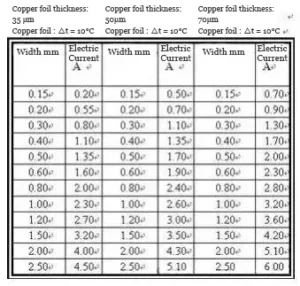
Note: i.When you use copper foil as conductors for high currents, you should derate the table values by 50% to select the copper-foil width for current carrying.
i i.In PCB design and manufacturing, engineers commonly use ounces (oz) as the unit for copper-foil thickness.
1 oz copper means the copper foil weighs 1 oz per square foot, and it corresponds to a physical thickness of 35 μm; 2 oz copper corresponds to 70 μm.
How to Determine the Width of High-Current Conductors
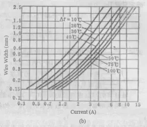
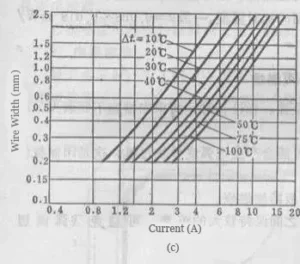
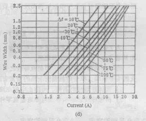
(b) Wire thickness: 35μm (c) Wire thickness: 70μm (d) Wire thickness: 105μm
Using PCB TEMP Software to Calculate(Calculate line width, current, impedance, etc.)
(Calculate line width, current, impedance, etc.)
PCBTEMP software: Enter the following in sequence:
Location (External/Internal) – whether the trace is on the surface or inside the FR-4 board
Temp – Temperature (Degree C)
Width – Line width (Mil)
Thickness – Thickness (Oz/Mil)
Then click Solve to determine the current passing through. Alternatively, given the current, you can calculate the line width. Extremely convenient.
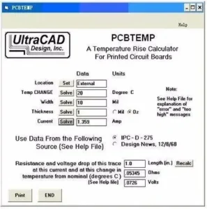
The results are similar to those obtained with the first method (20°C, 10 mil line width, equivalent to 0.010 inch line width, with a copper foil thickness of 1 oz).
Empirical Formula
Empirical Formula: I=KT0.44A0.75
(K is the correction factor; typically 0.024 for copper-clad laminate in inner layers and 0.048 for outer layers; T is the maximum temperature rise in degrees Celsius (copper’s melting point is 1060°C);
A is the copper-clad cross-sectional area in square mils (not square millimeters, note: square mil); I is the maximum allowable current in amperes (A).
Generally, 10 mil = 0.010 inch = 0.254 mm corresponds to 1 A; 250 mil = 6.35 mm corresponds to 8.3 A.
A Calculation Method Provided by A Netizen
First, calculate the cross-sectional area of the track. Most PCB copper foil has a thickness of 35μm (if uncertain, consult the PCB manufacturer).
Multiply this by the line width to obtain the cross-sectional area, ensuring conversion to square millimeters.
An empirical current density value of 15–25 amperes per square millimeter is applied. Multiplying this by the cross-sectional area yields the current-carrying capacity.
Some Experience Regarding Trace Width and Via Fill
When designing PCBs, we generally follow a common practice: use thicker traces (e.g., 50 mil or larger) for high-current paths, and thinner traces (e.g., 10 mil) for low-current signals.
However, in certain electromechanical control systems, instantaneous currents exceeding 100A may flow through traces. In such cases, thinner traces will inevitably fail.
A fundamental rule of thumb is 10A per square millimeter: a trace with a cross-sectional area of 1 square millimeter can safely handle 10A.
If the trace is too narrow, it will burn out under high current. Of course, current-induced trace burnout follows the energy formula: Q = I²t.
For example, a trace rated for 10A can withstand a sudden 100A current spike lasting microseconds. (This raises another issue: the trace’s stray inductance.
This spike will generate a strong counter-electromotive force due to this inductance, potentially damaging other components.
Thinner and longer traces have greater stray inductance, so practical design must also consider trace length comprehensively).
Trace Patterns and Their Impact on Current and Heat
Most PCB design software offers several options for routing vias around component pads: right-angle radiating traces, 45-degree radiating traces, or straight traces.
What’s the difference? Beginners often overlook this, choosing randomly based on aesthetics.
This is unwise. Two key considerations are: preventing excessive heat dissipation and ensuring adequate current-carrying capacity.
The straight pattern offers exceptional current-carrying capacity, making it essential for device pins in high-power circuits. It also provides strong thermal conductivity.
While beneficial for device cooling during operation, this poses challenges for PCB assembly personnel.
The rapid heat dissipation makes solder wetting difficult, often requiring higher-wattage irons and elevated soldering temperatures, thereby reducing production efficiency.
Choosing Pad Structures for Current and Thermal Balance
Using right-angle or 45-degree radiating pads reduces the contact area between the pin and copper foil, slowing heat dissipation and making soldering much easier.
Therefore, the choice between direct copper plating or via-through pads should be based on the application, balancing both current-carrying capacity and heat dissipation capabilities.
Direct copper plating should be avoided for low-power signal lines, while it is essential for pads carrying high currents.
The choice between right-angle or 45-degree pads is primarily aesthetic.

