Since radio frequency (RF) circuits are distributed-parameter circuits, skin effect and coupling effects are likely to occur during actual circuit operation.
Therefore, in practical PCB design, it is often difficult to control interference radiation within the circuit, such as mutual interference between digital and analog circuits, noise interference from power supplies, and interference caused by improper grounding.
For this reason, the key to successful RF circuit PCB design lies in trade-off evaluation throughout the design process.
Designers need to find a proper balance. This helps minimize such interferences to the greatest extent.
It can even eliminate interference in partial circuit sections.
This article provides some design techniques from a PCB layout perspective that are highly effective in improving the interference immunity of RF circuits.
RF Layout
This section primarily discusses the placement of components on multilayer boards.
Component placement has core requirements for RF layout. Components on the RF path shall be arranged with optimized orientation.
This minimizes the physical length of the RF path. Isolation between input and output must be maintained.
High-power circuits should be separated from low-power circuits as far as possible.
Sensitive analog signals need to be kept away from high-speed digital signals and RF signals.
The following techniques are commonly used in layout design.
In-Line Layout
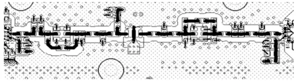
Components for the RF main signal should be arranged in an in-line layout whenever possible, as shown in Figure 1.
However, due to space constraints on the PCB and within the enclosure, an in-line layout is often not feasible. In such cases, an L-shaped layout may be used;
It is best to avoid a U-shaped layout (as shown in Figure 2). If a U-shaped layout is unavoidable, maximize the distance between the input and output to at least 1.5 cm.
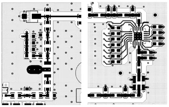
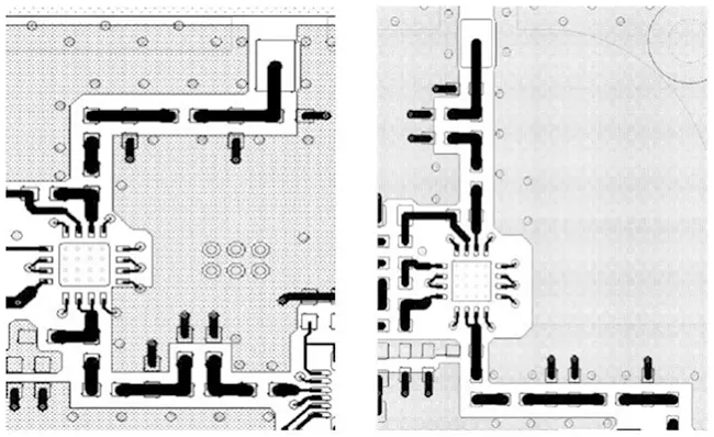
Additionally, when using an L-shaped or U-shaped layout, it is best not to turn immediately after entering the junction, as shown on the left in Figure 3, but rather to turn after a short straight section, as shown on the right in Figure 3.
Identical or Symmetrical Layouts
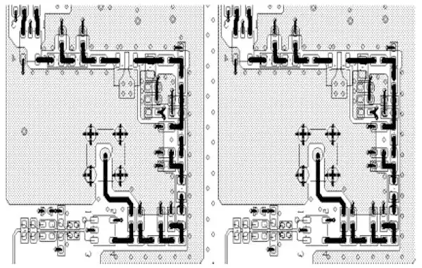
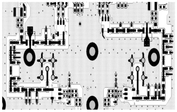
Identical modules should be arranged in identical or symmetrical layouts whenever possible, as shown in Figures 4 and 5.
Cross-Shaped Layout
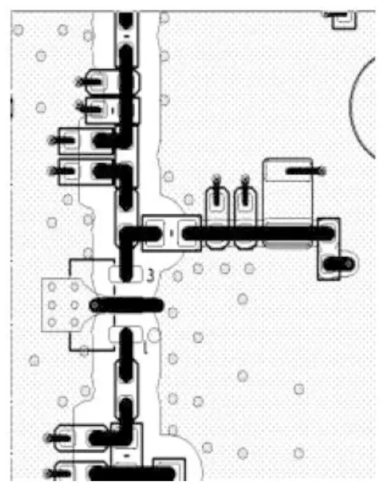
In an offset circuit, the feed inductor is positioned perpendicular to the RF path, as shown in Figure 6, primarily to avoid mutual inductance between inductive components.
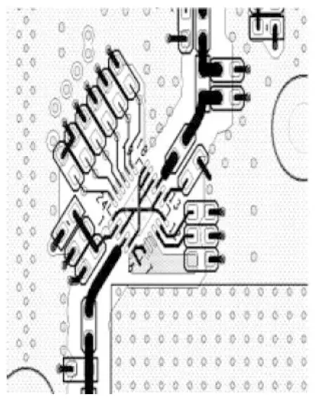
45-Degree Layout
To make efficient use of space, components can be arranged at a 45-degree angle to keep the RF lines as short as possible, as shown in Figure 7.
RF Routing
There are general requirements for routing. RF signal traces shall be kept short and straight.
Abrupt changes in trace direction should be minimized. The number of vias should be reduced as much as possible.
Crossing with other signal traces needs to be avoided. Add sufficient ground vias around RF signal traces.
The following are some common optimization techniques:
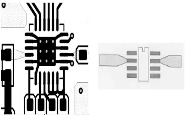
Gradient Line Design
When the width of the RF lines is significantly greater than that of the IC device pins, the line width connecting to the chip is designed with a gradient, as shown in Figure 8.
Arc-Shaped Bends
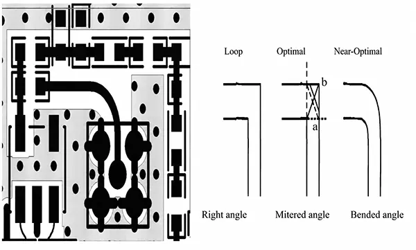
When an RF line cannot be laid straight, it should be bent into an arc. This reduces external radiation of the RF signal and mutual coupling.
Experiments have shown that using a curved right angle at the corners of a transmission line minimizes return loss, as shown in Figure 9.
Ground and Power
Use the thickest possible ground traces. Whenever possible, lay ground planes on every layer of the PCB and connect them to the main ground plane.
Use as many ground vias as possible to minimize ground impedance.
Avoid segmenting the power plane in RF circuits. A continuous power plane not only increases the radiation of RF signals from the power plane but also makes it more susceptible to RF interference.
Therefore, power traces or planes are generally designed in long, narrow strips.
Trace width shall be determined according to current load. Traces should be made as wide as possible to satisfy current carrying capacity.
However, unlimited widening of traces is not allowed. When routing power traces, avoid forming loops.
Power traces and ground traces should run parallel to the direction of the RF signal but must not overlap;
Where they cross, a perpendicular cross-over is recommended.
Crossing Routing
RF and IF signal traces should cross at right angles, with a ground plane inserted between them whenever possible.
When RF signals cross other signal traces, try to place a ground plane connected to the main ground along the RF trace between them.
If this is not possible, ensure that they cross at right angles. “Other signal traces” here also include power lines.
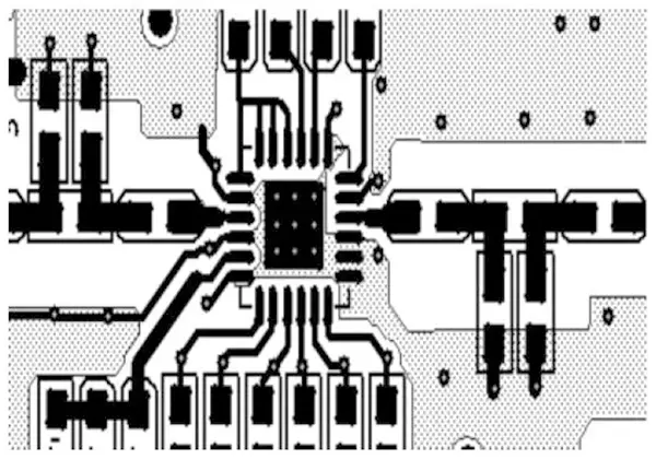
Ground Loop Processing
Ground loop processing is applied to radio frequency signals, interference sources, sensitive signals, and other important signals.
This not only improves the signal’s immunity to interference but also reduces the interference that the signal causes to other signals. As shown in Figure 10.
Copper Foil Processing
Copper foil must be smooth and flat; long lines or sharp corners are not permitted.
If they cannot be avoided, add several ground vias at the sharp corners, along the edges of long, narrow copper foil sections, or at the edges of the copper foil itself.
Spacing Guidelines
RF traces must be at least 3W away from the edge of an adjacent ground plane, and there must be no ungrounded vias within 3W of that edge.
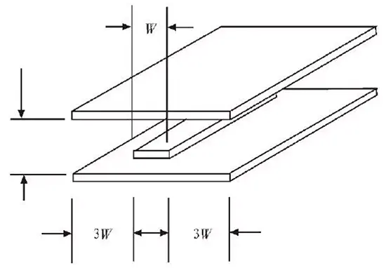
RF traces on the same layer must be surrounded by a ground plane, and ground vias must be added to the ground plane.
The spacing between vias should be less than 1/20 of the wavelength (λ) corresponding to the signal frequency, and they should be arranged uniformly and neatly.
The edge of the ground plane should be 2W in width or 3H in height away from the RF trace, where H represents the total thickness of the adjacent dielectric layers.
Enclosure Design
For the entire RF circuit, the RF units of different modules should be isolated from one another using enclosures, particularly between sensitive circuits and strong radiation sources.
In high-power multistage amplifiers, isolation between stages must also be ensured.
Once the entire circuit has been properly laid out, the next step is to design the shielded enclosures.
The following precautions should be observed when designing shielded enclosures:
The entire shielded cavity should be designed as regularly shaped as possible to facilitate casting.
Each shielded cavity should ideally be rectangular; square shielded cavities should be avoided.
The corners of the shielded cavity should be rounded. Since shielded metal cavities are typically cast, rounded corners facilitate the removal of the casting from the mold during the casting process, as shown in Figure 12.
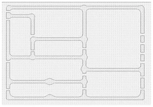
The perimeter of the shielded chamber is sealed. Cables are typically routed into the chamber using stripline or microstrip, while microstrip is used to connect different modules within the chamber.
Where different chambers are connected, a 3-mm-wide slot is cut, with the microstrip running exactly down the center.
3-mm metallized holes are placed at the corners of the cavity to secure the shielding housing.
An equal number of metallized holes are also evenly spaced along each long side of the cavity to provide additional structural support.
The cavity is typically provided with openings to facilitate soldering of the shielding housing.
The cavity wall is generally at least 2 mm thick and features two rows of window vias, which are staggered relative to each other, with a spacing of 150 mil between vias in the same row.
Conclusion
The key to the success or failure of RF circuit PCB design lies in minimizing circuit radiation to improve immunity to interference.
However, in actual layout and routing, addressing certain issues often involves trade-offs.
Therefore, designers must consider how to find a balance that optimizes the overall performance of the RF circuit.
All of this requires designers to possess a certain level of practical experience and engineering design skills.
However, acquiring these abilities cannot happen overnight for any designer; only by learning from others’ experiences and combining them with one’s own continuous exploration and reflection can one make steady progress.
This article summarizes some design experiences gained through practical work, which can help improve the interference immunity of RF circuit PCBs and assist beginners in RF circuit design in avoiding unnecessary detours.