PCB step slots, also known as controlled-depth slots or non-through slots, are recessed grooves milled into specific layers within a PCB board without penetrating the entire board. Imagine them as “pits” dug between the “floors” of the PCB.
Unlike V-cuts (stamp holes) or standard through-slots that penetrate the entire board thickness, the depth of a step slot is precisely controlled.
It removes only the specified number of layers of substrate and copper foil while preserving the integrity of the other layers.
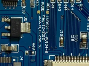
As shown below, excerpted from IPC-6012F
★ Key Characteristics of Step Slots
Non-penetrating: Does not extend through the entire PCB.
Controllable depth: Typically defined as “milled to layer X” or a specific depth value.
Unplated or plated sidewalls: Slot inner walls expose the substrate or are copper-plated.
★ Step Slot Classification
IPC-6012F defines three types:
- Type 1 – Step slot bottom or sidewalls lack metallization
- Type 2 – Step slot bottom or sidewalls have metallization, but not simultaneously
- Type 3 – Step slot bottom and adjacent sidewalls have continuous plated metallization

★Primary Applications of Step-Down Slots
Step-down slots are primarily designed to address complex challenges involving space constraints, assembly requirements, and signal integrity.
Component Embedding
Scenario: To reduce overall assembly height and achieve slimmer product designs. This involves placing taller components (e.g., chips, connectors, capacitors) within step-down slots so their tops do not protrude above the PCB surface.
Applications: Smartphones, wearable devices, high-density modules.
Auxiliary Connector/Module Mounting
Scenario: Mounting another PCB sub-board or FPC (Flexible Printed Circuit) onto the main board in a parallel, overlapping configuration with extremely tight spacing requirements. Step grooves are cut at corresponding positions on the main board.
The sub-board’s gold fingers or connectors are inserted and seated within these grooves, then secured via screws or soldering. This provides greater stability and space efficiency compared to simple board-to-board connectors.
Enhanced Thermal Management
Scenario: Certain high-power components require direct contact with the enclosure or heat sink.
This involves creating stepped slots beneath the component to allow thermal pads or thermal grease to be directly filled into the slots.
This ensures tighter contact between the component’s housing or base island and the external heat dissipation path, reducing thermal resistance.
Specialized Electromagnetic Shielding
Scenario: Creating isolated cavities in specific PCB areas is required. By machining stepped grooves at the shielding cover’s mounting location, the cover’s “walls” can be embedded within the grooves, providing enhanced mechanical stability and shielding continuity.
Prevent Component Interference
Scenario: A component with significant height is mounted on one side of the board, while another component must be installed at the corresponding position on the opposite side.
Machining a stepped groove on Side A creates clearance for the component on Side B, preventing structural interference.
★Manufacturing Process for Step Grooves
For Type I step grooves manufactured during the later stages of PCB production—typically after through-hole plating and either before or after outer layer circuit formation (depending on specific design)—the following process description applies.
1. PCB Laminating and Via Formation
Standard processes for multilayer boards—lamination, drilling, and via plating—are completed first.
2. Fixturing and Alignment
The PCB is secured to a CNC milling machine.
3. Depth Reference Calibration
The milling machine measures the PCB surface height using a probe or laser, establishing the “zero plane” for milling.
4. Depth-Controlled Milling
Milling is performed using a specific cutter based on preset depth data.
The cutter rotates at high speed, progressively removing the overlying dielectric material (e.g., FR-4) and copper foil layer by layer until the specified depth is reached.
Multiple milling passes may be required to ensure slot bottom flatness and depth accuracy.
5. Post-Milling Cleaning and Deburring
Cleaning and Deburring After milling, debris and copper burrs within the slots are removed using high-pressure water jets, brush grinding, or plasma cleaning. This is a critical step for ensuring reliability.
6. Post-Processing: Solder Mask and Surface Finishing
Subsequent Processes Subsequent processes such as solder mask application and surface finishing (e.g., electroless gold plating, tin spraying) are then performed.
Alternatively, depth-controlled milling may be performed after surface finishing, depending on design and manufacturing requirements.
★ Inspection Standards for Step Grooves
Inspection requirements are defined in IPC-6012F as follows:
Step grooves shall meet design dimensional requirements (e.g., length, width, depth, and location).
Unless otherwise specified, final surface coating thickness requirements in Table 3-3 shall be based on measurements from the outer layer.
For Type 1 step grooves, the following conditions shall be met:
♦ Type 1 Step Grooves Requirements
- The groove bottom appearance shall be visually uniform and consistent.
- Exposed broken fibers shall comply with the requirements of Section 3.3.2.6.
- Non-bonded gaps (not delamination) caused by material misalignment, reduced prepreg material, etc., may retract to a maximum of 50% of the distance from the groove edge sidewall to the nearest conductor, or 0.25 mm [0.010 in], whichever is smaller.
- Requirements for destructive physical analysis (DPA) to verify observed non-bonded gaps shall be mutually agreed upon by the supplier and customer.
For Type 2 stepped slots, the following conditions shall be met:
♦ Type 2 Stepped Slot Requirements
- For conductors in stepped slots that are continuous in the plane and protrude from the slot wall, adhesive flow onto the conductor element shall not exceed 0.75 mm [0.0295 in].
- The allowable adhesive flow for connection pads located within 0.75 mm [0.0295 in] of the slot wall at the bottom of a stepped slot shall be determined by mutual agreement between the supplier and the customer.
- Non-bonded gaps (not delamination) caused by material misalignment or reduced prepreg material may retract to a maximum of 50% of the distance from the slot edge sidewall to the nearest conductor, or 0.25 mm [0.010 in], whichever is smaller.
- Requirements for destructive physical analysis (DPA) to verify non-bonded gaps shall be mutually agreed upon by the supplier and purchaser.
For Type 2 and Type 3 stepped slots, the following conditions shall be met:
♦ Type 2 and Type 3 Stepped Slots – Coating and Plating Requirements
- Unless otherwise specified in the procurement documents, the intact area of the conductor element requiring solder or wire bonding coating at the slot bottom, excluding the permitted adhesive flow area, is defined as the area within 60% of the element contour (circular, rectangular, square, etc.) center and shall meet the process requirements of Section 3.5.4.
- For Type 2 and Type 3 stepped grooves with plated walls, when visually inspected (non-microscopic sectioning) per Section 3.3, voids in the wall plating and coating shall not exceed the allowable limits specified in Tables 3-6.
- Each plated wall of a stepped groove shall be evaluated individually; the cumulative area of multiple voids on the same side wall shall not exceed the specified percentage area.
★ Advantages & Disadvantages
Advantages
Space savings: One of the ultimate means to achieve ultra-high-density assembly.
Enhanced mechanical stability: Embedded installation provides greater security than surface mounting.
Optimized thermal dissipation and shielding performance.
Increased design flexibility: Resolves complex structural interference issues.
Disadvantages and Challenges
High cost: Adds complex processing steps with stringent equipment and process requirements, potentially impacting yield rates.
Process complexity and precision control challenges: Tolerance control for depth and shape is difficult.
Residual Debris: Incomplete cleaning may cause short circuits.
Laminate Delamination Risk: Milling may compromise bond strength of remaining layers, potentially leading to delamination under thermal stress.
Stress Concentration: Sharp corners of milled slots can become focal points for mechanical stress.
Design Complexity: Requires highly precise design and thorough communication with PCB manufacturers.
PCB step grooves represent an advanced, high-end PCB process designed to address extreme space and structural challenges.
They hold irreplaceable value in fields such as consumer electronics, communications, and aerospace.
However, adopting this technology requires weighing its high cost and potential technical risks.