Sonar plays a crucial role in marine exploration and national defense, and printed circuit boards (PCBs) are one of its core components; therefore, the quality of PCBs directly affects the performance of sonar systems.
Sonar systems must meet both high-frequency and wide-bandwidth requirements; coupled with the high pressure and salt corrosion issues in deep-sea environments, the manufacturing process for their PCBs is extremely challenging.
In recent years, sonar technology has continued to advance and its applications have expanded, yet PCBs for these systems still face challenges such as high-frequency signal loss and signal instability.
This paper analyzes these challenges from three perspectives: material selection, structural design, and manufacturing processes.
The aim is to improve the performance and reliability of sonar circuit PCBs.
Additionally, it provides a reference for other underwater electronic devices.
Basic Principles and Design Requirements of Sonar Circuits
How Sonar Circuits Work
The composition of the sonar system modules is shown in Figure 1. Figure 1 illustrates the core functions of each module and the key requirements for the PCB.

1. How Sonar Systems Work
In a sonar system, the transmitter circuit first generates an electrical signal, which is then converted into sound waves by the transducer and emitted.
When these sound waves encounter a target, they are reflected back, forming an echo signal.
The transducer then receives the echo and converts it back into a faint electrical signal.
The receiver circuit amplifies and filters this signal, and finally, the signal processing circuit analyzes it to determine information such as the target’s distance and bearing.
2. Manufacturing Requirements for Sonar System PCBs
① Transmitter Circuit: Since this circuit must output high-power, high-frequency signals, materials with low dielectric loss should be used to minimize energy loss;
② Receiver Circuit: Surface acoustic wave (SAW) filters are sensitive to temperature, which can affect filtering performance; therefore, the PCB must meet thermal stability requirements;
③ Signal Processing Circuit: High-frequency broadband signals are susceptible to electromagnetic interference, making grounding design and shielding methods critical;
④ Environment: In underwater, humid, or corrosive environments, surface treatments must provide moisture resistance and corrosion resistance.
In summary, material selection, layer stacking design, and manufacturing processes must be comprehensively considered to ensure the performance of the entire system.
Design Requirements for Sonar Circuits
When designing sonar circuits, it is essential to focus on three key parameters: signal integrity, electromagnetic compatibility, and thermal management.
These factors directly impact the detection accuracy and operational stability of the sonar system. Each aspect involves critical issues, design considerations, and primary factors.
1. Signal Integrity
In terms of signal integrity, the underwater acoustic signals processed by sonar circuits are generally weak and span a wide frequency range; in the high-frequency range, signal attenuation and distortion are common issues.
For example, in the hardware circuit design of a single-beam imaging sonar system, it is essential to ensure that important information is not lost during the transmission of weak signals at the receiving end.
This requires PCB manufacturing processes to minimize the length of high-frequency signal lines during routing.
It also involves employing equal-length routing and impedance matching designs.
Additionally, substrate materials with stable dielectric constants should be selected to reduce signal reflections and losses during transmission.
2. Electromagnetic Compatibility
Electromagnetic compatibility is another critical aspect of sonar circuit design.
Sonar systems typically include both transmitter and receiver modules, and the high-power signals from the transmitter can easily interfere with the sensitive circuits in the receiver.
In towed active sonar systems, circuit modules are densely packed into a small space, resulting in a complex electromagnetic environment.
To address this issue, PCB manufacturing processes must employ sound grounding design practices.
This includes incorporating dedicated ground planes and shielding layers.
It also involves separating digital and analog circuits to prevent interference signals from affecting each other through common impedance.
Additionally, in multilayer board designs, electromagnetic shielding effectiveness can be enhanced by increasing the number of ground layers and optimizing the spacing between layers.
3. Thermal Performance
Thermal performance is critical for sonar systems operating over extended periods.
Circuit components generate significant heat when operating at high power; inadequate heat dissipation can degrade component performance or even cause failure.
Key components such as surface acoustic wave (SAW) filters are highly sensitive to temperature changes; rising temperatures can cause a shift in their center frequency, affecting the stability of the sonar system’s operating frequency.
Therefore, PCB design must incorporate features such as large copper-clad areas and heat-dissipating vias to enhance heat conduction.
Additionally, substrate materials with high thermal conductivity should be selected, and when necessary, heat sinks can be mounted on the PCB or a metal enclosure can be used to aid in heat dissipation.
Through material selection, optimized layout and routing, and structural design, PCB manufacturing processes can meet the design requirements of sonar circuits.
These requirements include signal integrity, electromagnetic compatibility, and thermal management.
By doing so, they lay the foundation for the reliable operation of sonar systems.
Key Technologies in Printed Circuit Board Manufacturing
Material Selection and Characteristic Analysis
The choice of material for sonar circuit PCBs directly determines whether the signal transmission is smooth and whether the board can withstand the underwater environment.
A common, inexpensive material is flame-retardant glass-epoxy (FR-4).
While a single board doesn’t cost much, its dielectric constant (Dk) fluctuates at higher frequencies, with a variation of approximately 4.4±0.2;
The dielectric loss (Df) reaches 0.02, causing a portion of the waveform to be clipped and the phase to shift, resulting in inaccurate measurement data.
In contrast, polytetrafluoroethylene (PTFE) is much more stable: its Dk remains steady at 2.1 with almost no variation, and its Df is below 0.001.
It effectively retains high-frequency energy and is commonly used in the front-end circuits of broadband transducers.
There are two types of copper foil used. The first has an electrolytic roughness of about 1.5 µm, where high-frequency currents travel close to the surface and the roughness dissipates energy.
The second has a calendered roughness of less than 0.5 µm, which has lower losses and performs better in current signal paths for towed sonar.
PTFE offers the best performance but is also the most expensive; Rogers RO4350 falls in the middle, with Dk = 3.66 and Df = 0.004.
Its performance and cost are both acceptable, making it commonly used in standard mid-range sonar models.
Therefore, if high-frequency and long-range detection are required, PTFE with laminated copper foil is the preferred choice.
However, if the focus is on mid-to-low frequencies and cost savings, high Tg modified FR-4 with electrolytic copper foil is also a viable option.
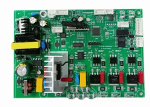
Design and Manufacturing Processes for Multilayer PCBs
The key aspects of the multilayer PCB process for sonar circuits are shown in Figure 2.
These include their primary functions, impedance matching issues, and lamination process parameters.
The figure also highlights existing limitations, as well as future development directions and optimization methods.
Figure 2 clearly illustrates the relationships among these aspects.

1. Interlayer Trace Routing
In sonar circuits, a multilayer PCB is like a stack of roads; when routing traces between layers, the primary paths are established first.
The transmit signal channel is placed on the inner layer of the second layer, the receive signal channel on the inner layer of the third layer, with a complete ground plane sandwiched in between.
The 40 kHz and 200 kHz analog differential lines are arranged side by side, with a line width of 0.11 mm and a spacing of 0.15 mm.
The measured differential impedance is 98 Ω, which is essentially identical to the transducer’s resonant impedance (98 Ω ±5%); the echo loss is 22 dB, a reduction of approximately 6 dB compared to a random line layout.
2. Impedance Matching Design
Adjustments were made based on three factors: “copper thickness, dielectric material, and layer stacking order.”
The outer copper foil thickness was reduced to 18 μm; FR-4 Tg170 dielectric material with a thickness of 0.1 mm was selected; and the layer stacking order was set to signal-ground-signal-power-ground.
The total thickness of the five-layer board is 1.0 mm. At 1 GHz, with a Dk of 4.3, calculations show that a microstrip line width of 0.10 mm yields a single-ended impedance of 50 Ω, with an error of ±3%.
This reduces reflection peaks by 40% compared to conventional 1.6 mm thick boards.
3. Grounding Design
The grounding design employs a “well” pattern of through-hole walls: a 0.25 mm diameter hole is drilled every 5 mm along the board edges.
The inner-layer ground network is directly connected via these holes, forming a loop inductance of 0.3 nH, which limits common-mode interference to −85 dBm, meeting the towed sonar’s sensitivity requirement of −80 dBm.
4. High-Density Interconnect Design
In the high-density interconnect (HDI) section, Type 1–3 matching layer circuits are embedded within laser-drilled holes.
The holes are first filled with 1067PP material, and then drilled into 0.075 mm micro-blind vias.
These vias have a copper thickness of 12 μm inside the holes and a maximum depth of 5 μm.
The finished product exhibits an insertion loss of only 0.8 dB at 320 kHz, is 0.4 mm thinner than a standard through-hole board, and saves 15% in area, making it a perfect fit for a 70 mm diameter ceramic heat sink.
5. Manufacturing Process
Manufacturing steps: Material cutting → Inner layer pattern formation → AOI inspection → Browning treatment → Multilayer lamination → Laser drilling → Chemical copper plating → Via filling → Outer layer pattern formation → Solder mask application → Chemical gold plating → Testing.
During lamination, the temperature is 185°C and the pressure is 3.5 MPa.
The cooling rate during cold pressing must not exceed 3°C/min to ensure no air bubbles form at the interface between the FR-4 and PP materials.
Actual testing showed that after 100 temperature cycles ranging from −40°C to +85°C, the resistance change rate was less than 2%, meeting the requirement for five years of maintenance-free operation in deep-sea imaging sonar applications.
Conclusion: This simple method first separates the frequencies between layers and then shares a common ground.
It also accurately calculates impedance in a single step and fills the blind vias in the HDI.
By doing so, it reduces stray echoes in the sonar circuit’s multilayer board by an additional 4 dB.
In addition, it increases the mass production yield rate from 85% to 96%.
Optimization of Manufacturing Processes for Sonar Circuit PCBs
Process Assurance for Signal Integrity
Signal integrity in sonar circuits significantly impacts the accuracy of detection results and system stability.
Optimizing PCB layout, routing, and shielding processes can help reduce interference and attenuation of high-frequency signals.
Based on fundamental theories of electromagnetic fields and relevant transmission line models, specific methods for ensuring the quality of these processes will be discussed below.
1. Layout
PCB layout should minimize the path length of high-frequency signals and isolate sources of interference.
Transmit and receive modules should be placed on opposite sides of the board.
Separate power and ground planes should also be used to avoid coupling noise caused by a shared ground.
High-power components should be placed away from circuits that receive low-level signals; isolation slots should be added when necessary;
Grounding should follow the single-point grounding principle, with the digital and analog ground planes connected via ferrite beads or zero-ohm resistors.
An example involving a deep-water imaging sonar demonstrated a 12 dB reduction in background noise after optimization.
2. Wiring
When routing signals, ensure impedance continuity and prevent signal interference:
For signals in the MHz to GHz range used in sonar circuits, microstrip or stripline must be used to achieve 50 Ω or 75 Ω impedance matching;
Differential signal lines should be routed in parallel with equal lengths to minimize phase distortion; traces on adjacent layers should be oriented perpendicular to each other.
When the spacing between traces is three times the trace width, crosstalk can be reduced to less than 15% of its original value.
3. Shielding
Shielding is a key method for addressing electromagnetic interference. Multilayer boards should incorporate a complete ground shielding layer to enclose signal layers that are susceptible to interference.
Critical circuits, such as high-speed clock lines, should be wrapped in copper foil or enclosed in a metal shield.
There is also a technology known as frequency-selective surfaces (FSS), made of flexible liquid metal, which can dynamically adjust the shielding frequency band.
In a towed active sonar project, the signal-to-noise ratio was improved by approximately 8 dB through a combination of current-mode transmission and shielding optimization.
4. Results
Comparative results from HFSS simulations show that, following optimization, the S11 parameter value for the critical network decreased by 40%, and far-end crosstalk (FEXT) was reduced by 35%;
Actual measurements of a 1 MHz pulse propagating through a 10-layer HDI board showed that attenuation decreased from −3.2 dB to −1.8 dB, and waveform distortion improved by 22%.
Signal quality can be enhanced through process optimizations such as PCB layout, routing, and shielding.
Future research should focus on the application of nano-coated shielding materials and heterogeneous integration processes in ultra-high-frequency sonar systems.
It should also address the long-term stability of shielding structures under deep-sea high-pressure conditions.
Improved Reliability and Environmental Adaptability
Once a sonar circuit PCB is deployed in the deep sea, it is constantly exposed to a humid, high-pressure, and saline environment, conditions that directly shorten its service life.
Moisture first penetrates the board; as the insulating material absorbs water, its dielectric constant (Dk) decreases, and leakage current increases accordingly.
High pressure can also cause the adhesive joints between layers to separate, potentially causing the board to bulge or even crack.
The combined action of salt particles and other chemicals in seawater causes copper traces to rust and turn green rapidly; once electrochemical migration occurs, the circuits will break.
If the signal becomes corrupted, the sonar system may suddenly cease to function.
Need for Enhanced PCB Protection
Therefore, the PCB must first be made robust enough to withstand these environmental conditions, ensuring the system has a longer service life.
Two protective measures can be implemented: improving surface treatment and adding a protective layer.
Instead of using hot-air leveling solder, the surface is treated with electroless nickel immersion gold (ENIG).
The nickel layer first covers the copper. Phosphorus is mixed in to stabilize the nickel layer and prevent corrosive substances from penetrating.
The thin gold layer on top ensures that solder can adhere to the joints during assembly.
Advanced Protective Coating: Parylene HT
For the protective layer, modified poly(p-xylene) (Parylene High Temperature, Parylene HT) as the protective layer.
By vaporizing it under vacuum, the material can coat every three-dimensional corner of the board.
The film is free of pinholes, has uniform thickness, extremely low moisture permeability, and stable chemical properties—much like slipping a transparent plastic protective shell over the board.
Compared to traditional conformal coatings, this film is less prone to rupture under high water pressure in the deep sea and will not loosen over time.
Comparative Testing and Validation
Two small signal boards were fabricated for comparative testing.
One was fabricated using the traditional method, while the other used ENIG with Parylene HT.
In accordance with the GJB 150.11A—2009 salt spray standard, the boards were continuously sprayed with a 5% saline solution at 35°C for 96 hours.
The board made using the traditional method developed green spots on the copper surface after 48 hours, and the pads began to rust; the impedance meter immediately triggered an alarm.
The board produced using the new method remained clean on the surface, and the film remained intact under electron microscopy.
The impedance change in critical circuits was less than 5%, and the insulation performance was maintained at 10¹² Ω.
High-Pressure Reliability Testing
The sample was then placed in a pressure chamber simulating a water depth of 3,000 m and subjected to 30 MPa of pressure for 72 hours.
The results showed that the edges of the boards made using the old process peeled off, while the film on the new boards remained firmly adhered, with no delamination or flaking.
The data indicates that combining the two protective measures significantly improved the boards’ durability.
Two issues require further attention: (1) whether the film will peel during thermal cycling; and (2) how long performance will remain stable after 1–2 years of actual deployment in the deep sea—further data collection is needed.
Case Study Analysis
We will use a PCB designed for a deep-sea sonar transmitter circuit as an example. Operating at a frequency of 150 kHz, it can deliver a peak power of 2 kW.
The board consists of eight layers, constructed by laminating FR-4 material with high-speed materials.
The signal layers use high-frequency materials with a dielectric constant (Dk) of 3.48 and a loss tangent (Df) of 0.0037 to retain high-frequency energy;
The power plane uses standard FR-4 material to reduce costs.
The heat generated by high power and warping issues in the 8-layer board were the most challenging problems to solve.
Factory implemented three measures
First, the traces carrying high currents were replaced with 70 μm copper foil, followed by copper plating.
The actual measured copper thickness was 105 μm, increasing the current-carrying capacity by 40%;
During lamination, the copper foil was arranged in a symmetrical 1-2-2-1 pattern; the board was first baked at 120°C for half an hour before being heated to 180°C, resulting in warpage controlled to 0.7%;
A small groove was machined in the high-voltage area and filled with thermal grease, reducing the thermal resistance to 1.2 °C/W.
Test results showed that during full-load operation, the PCB surface temperature rose by only 32 °C (compared to 51 °C previously), and harmonics dropped from 1.8% to approximately 0.9%;
When measured with a network analyzer, the 50 Ω trace exhibited return loss below −25 dB, and the PCB operated continuously for 500 hours under 60 MPa water pressure without failure.
This example demonstrates that laminating high-frequency materials with standard materials, combined with minor thermal management techniques, can indeed enhance PCB stability.
Remaining Challenges: Lamination Accuracy
However, achieving precise alignment during lamination becomes challenging. X-ray inspection revealed a layer misalignment of 75 μm, exceeding the specified tolerance of 50 μm.
This resulted in impedance fluctuations of approximately 5 Ω at the edges, which will pose obstacles when operating at higher frequencies.
To further increase the operating frequency, it is essential to improve the accuracy of alignment during lamination.
Therefore, for sonar circuit boards operating at frequencies exceeding 1 MHz, it is recommended to use AMB ceramic substrates, as the thermal expansion coefficients of ceramic and the chips are similar, minimizing misalignment during lamination.
It is also advisable to establish a failure database specifically for sonar circuit PCBs, quantifying issues such as thermal cycling cracks and electromigration into design benchmarks.
This will provide a data reference for the production of highly reliable sonar circuit PCBs in the future.
Conclusion
This paper investigates the process optimization of sonar circuit PCBs.
Based on the principles of acoustic detection, relevant theories of electromagnetic fields, and knowledge of electronic materials, it discusses process methods that meet the design requirements of sonar circuits.
Key Technical Points
To this end, three key technical points are proposed:
① Selecting substrate materials with low loss at high frequencies is crucial, as Dk and Df directly affect signal transmission speed and accuracy.
Practical testing has shown that selecting the right materials can reduce insertion loss by more than 15%;
② The combined application of HDI technology and precise impedance control can reduce interference in complex sonar circuits.
This is achieved through improvements in PCB layer design, routing methods, and grounding techniques.
It also ensures more complete signal transmission in confined spaces.
③ Given the unique conditions of the marine environment, enhancing the protective effects of PCB surface coatings, such as electroless nickel-gold plating or thick gold plating, can effectively resist corrosion.
Triple-proof coatings can also help protect against damage from humidity and salt spray.
Although the process optimization methods described in this paper have proven effective in many sonar products, it is important to understand that their application scope is still limited by existing materials and manufacturing precision.
Key Challenges
Future development of sonar circuit PCB processes must address two key challenges:
First, there is a need to develop new composite materials that exhibit minimal loss at high frequencies, strong heat resistance, and the ability to withstand harsh environments.
Examples include high-frequency resin materials reinforced with ceramic fillers or specialized substrates capable of operating in deep-sea high-pressure environments;
Second, artificial intelligence algorithms must be integrated with automated inspection equipment.
This will enable the timely detection of defects during production and the automatic adjustment of process parameters, thereby improving the yield and stability of complex multilayer PCBs.
Only through continuous research and development of new materials and the advancement of smart manufacturing technologies can we provide reliable processes for the next generation of high-performance sonar systems.