PCB silkscreen is a critical layer in printed circuit board (PCB) design that provides essential information for assembly, testing, and troubleshooting.
It primarily consists of text, symbols, and component markings that indicate orientation, polarity, and part identification.
Properly designed silkscreens ensure that PCBs are easy to assemble, verify, and maintain, while also improving overall product reliability.
What is PCB silkscreen?
PCB silkscreen primarily consists of text-based information, including circuit points, components, and circuit symbols.
The silkscreen layout varies depending on the PCB’s dimensions. If space is limited, priority should be given to the most critical information.

PCB silk screening primarily includes the following:
- Component reference marks
- Polarity marks
- Pin 1 marks
- Component boundaries
- Company logo
- Manufacturer’s mark
- Warning symbols
- Part number
- Version number
- Date code

The Complete Screen Printing Process
Screen Printing Design
Design the screen printing layers using EDA software.
This includes identifying and assembling all necessary markings, symbols, and text required for the components on the PCB.
The design is then exported in a format compatible with the manufacturer’s equipment.

PCB Manufacturing
The PCB manufacturing process involves printing a layer of copper onto a substrate, drilling holes for components, and then etching away the excess copper to create a PCB, which can take various shapes and patterns.
A specialized screen printing process is used to apply the circuit pattern onto the copper layer.
Applications of Screen Printing
After a PCB is manufactured, the screen printing process is used to print the screen layer, which involves creating a stencil for the screen printing design.
The stencil is created by applying a photosensitive emulsion to the mesh to form the desired image.
Curing the Ink
After applying the screen-printed layer, the ink must be cured to ensure proper adhesion to the PCB substrate.
This is typically accomplished by exposing the PCB to high temperatures or ultraviolet light for a specified period of time.

Inspecting and Testing PCBs
Finally, inspect and test the PCB to ensure that the silkscreen layer has been applied correctly and that all required markings and symbols have been printed.
Errors and omissions in the screen printing process can lead to assembly errors or functional failures.
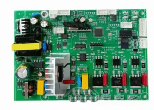
See the image below for a 3D view of a PCB with silkscreen printing:

Below is a 3D view of the PCB with the silkscreen layer removed.

It’s worth noting this difference; therefore, ensuring that PCBs are properly marked makes them easier to identify, thereby reducing the risk of errors during assembly and improving the overall reliability of the finished product.
PCB Silkscreen Design
Here are some important considerations for PCB silkscreen design:
Component Orientation and Polarity
The orientation markings on the silkscreen indicate the direction in which the component should be soldered; these are typically represented by dots, with the dot indicating pin 1 of the IC.
For LEDs and diodes, the markings are “+” or “C,” where “C” stands for cathode and ‘A’ for anode.
For capacitors, a half-shaded circle indicates negative polarity, while a “+” indicates positive polarity.

Overlapping Text
Edit the text orientation of component references, part types, and other elements to ensure they all face the same direction for easier reading.
You can also set top and bottom silkscreen text.
Before rotating text or adjusting component reference indicators, check for text overlap.
As shown in the figure below, the text directions are inconsistent and overlap.
This makes the text unusable as a reference during assembly and troubleshooting.
Therefore, when encountering such overlap during design, you must rotate and move the component reference indicators to the correct direction and position.

Check whether the component reference markers placed on the PCB pads overlap with the pads themselves.
As shown in the figure below, the first marker circled overlaps with the pad, making it unusable as a reference during assembly and troubleshooting.
Therefore, the marker must be moved to an empty space on the corresponding component.

Check the markings on the through-holes. Refer to the second component marking in the figure below.
Since through-holes without a mask cannot be printed, but when you use a solder mask to cover a through-hole, it cannot be used as a test point; it is best to move it to the side of the component.

Check to see if a reference marker has been placed so that, after the component is soldered, the marker is located beneath the object.
As shown below, if there is a marker beneath the component, move it to an empty space next to the component.

Additional Markers
Adding additional markers can help better indicate the orientation of components.
As shown in the figure below, in addition to the component’s original marker orientation, you can add markers in shapes such as triangles and circles to indicate the orientation of I/O components.

Place a polarity mark on the outside of the component, as shown in the figure below for a positive polarity mark.
Components with polarity, such as electrolytic capacitors, diodes, and LEDs, generally require this mark.

You can add measurement marks indicating the number of pins and traces on the IC via screen printing, as shown below:

Screen Printing Process
Selecting the appropriate screen printing process is critical, as the printing method will affect design parameters such as the dimensions, spacing, and placement of screen-printed elements on component pads, traces, and vias.

Appropriate Screen Printing Fonts
Choosing the right font ensures high readability, taking into account factors such as screen printing size, height, color, and font style.
The most common dimensions are 35 mil in height and 5 mil in stroke width, as well as 25 mil in height and 5 mil in stroke width.

Conclusion
In summary, PCB silkscreen plays a vital role in both the manufacturing and functional integrity of a PCB.
From precise screen printing and ink curing to careful placement of component markers and polarity indicators, attention to silkscreen design reduces errors, simplifies assembly, and enhances readability.
By following best practices in silkscreen layout and process, manufacturers can ensure that PCBs are both accurate and reliable.