
Before a new PCB assembly model enters mass production, it typically requires validation through multiple prototype versions.
Solder Paste Inkjet in PCB Assembly Optimization
The optimization and adjustments made to each prototype version inevitably result in changes to the component layout.
Limitations of Traditional SMT Stencil Printing
In modern electronic assembly, surface-mount components have replaced through-hole components as the mainstream.
Designers must create and manufacture an SMT stencil for each prototype version.
Over time, this leads to a massive number of stencils, keeping manufacturing costs high and occupying limited production space. PCBA prototype production schedules are often tight, while stencil fabrication generally takes 2–3 days, which can easily delay delivery.
Using stencils to apply solder paste to pads on PCBs with high-density, fine-pitch surface-mount components often causes problems.
These problems include poor printing accuracy, suboptimal solder paste formation, and frequent soldering defects.
Screen printing cannot be used to reapply solder paste to specific pads on a PCB, resulting in poor flexibility.
With small-batch, high-variety PCB assembly production now the norm, the current SMT screen printing model can no longer meet the need for rapid market response.
Research Focus: Solder Paste Inkjet Technology
To address these issues, this paper conducts a feasibility study on the application of solder paste inkjet printing technology and equipment in PCBA production.
First, engineers analyze the application based on a PCBA prototype production line.
They present a design proposal for a new production line. They also conduct a feasibility analysis.
Next, the study follows the trend toward miniaturization and precision in PCB assembly.
It evaluates the feasibility of applying solder paste inkjet technology to high-density, fine-pitch components.
The study also conducts validation tests for solder paste inkjet printing.
The production efficiency and procurement costs of solder paste inkjet equipment are analyzed.
The analysis leads to a new SMT production line design that integrates solder paste inkjet equipment with conventional screen printers to meet current production demands.
Engineers also develop a new design scheme for the PCB assembly repair process to tackle the challenges associated with PCB assembly repairs.
Ultimately, this initiative achieved cost reduction and efficiency gains in PCB prototype production, shortened processing cycles, significantly improved the quality of solder paste formation for high-density fine-pitch components, and substantially increased the first-pass yield rate for mass-produced PCB SMT soldering.
Solder Paste Dispensing Technology
Currently, in the surface mount assembly (SMT) process for PCBs—whether for prototype production or mass production—solder paste is applied using stencil printing.
However, as electronic components continue to become increasingly miniaturized and fine-pitch PCB technology becomes more widespread, the precision of stencil printing is no longer sufficient to meet soldering quality requirements.
This has become a bottleneck in production, leading to a significant increase in the defect rate on SMT production lines.
Advantages
Solder paste jetting technology overcomes the limitations of stencil printing, which often lacks precision, and meets the ultra-high-precision solder paste placement requirements for each solder joint.
Controlled by a high-resolution optical encoder and advanced software, solder paste jetting equipment equipped with a 3G acceleration drive system can move across PCBs at speeds exceeding 1 million dots per hour;
At the same time, integrated automatic PCB warpage compensation technology addresses the issue of solder paste printing offset caused by PCB warpage, enabling the equipment to not only operate at high speeds but also precisely control the volume and diameter of solder paste deposition.
This results in perfect solder joints after reflow soldering, ensuring excellent consistency in product quality.
Advanced Nozzle and Multi-Material Capability
The solder paste dispensing equipment utilizes advanced non-contact dual nozzles, allowing simultaneous dispensing of two solder pastes with different particle sizes to print on PCBs containing both high-density fine-pitch components and conventional components, enabling high-precision and flexible production of mixed-component PCBs.
High-Speed Dual-Track Production System
The solder paste printing equipment features a dual-track system. While one PCB is being printed, the next PCB is already loaded on the second track, ready for printing.
This enables seamless production between PCBs, thereby improving production efficiency.
Rapid Programming and Lean Manufacturing Compatibility
By importing the PCBA’s Gerber or CAD files into the solder paste printing equipment, the compilation of the printing format can be completed within minutes.
With minimal setup time and a high degree of automation, the system meets the requirements of lean manufacturing.
Precision Performance and Application Scope
The solder paste dispensing system achieves a single-point repeatability of ±35 μm, a single-point accuracy of ±40 μm, and a positional accuracy of 0.2 μm.
Thanks to precise solder paste dispensing, the amount of solder paste at each individual solder joint can be precisely controlled, making it widely applicable for FPC circuit boards, LED circuit boards, PCB cavities, and PoP (Package-on-Package) applications.
The high precision of the solder paste dispensing equipment enables it to meet the production demands of PCBAs involving high complexity, mixed assembly, mass production, and prototype manufacturing.
Principle
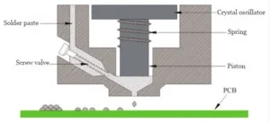
The print head and PCB board utilize a non-contact printing method. Once the print head height is set, the cantilever carrying the print head performs linear motion along the X and Y axes.
The cantilever has a maximum acceleration of 3g (approximately 30 m/s²).
Through advanced DSP servo motion control, high-speed flying-printing of solder paste is achieved.
A screw valve continuously feeds solder paste from the print cartridge into the ejection chamber, ensuring the chamber remains constantly filled with solder paste.
The piezoelectric driver consists primarily of a piezoelectric crystal, a high-performance spring, and a high-precision piston.
Its acceleration can reach 10,000 g, enabling the piezoelectric ejection valve to expel solder paste from the chamber at high speed.
The solder paste leaves the chamber in a controlled manner and lands on the PCB, as shown in Figure 1.
The breakpoint for the solder paste flow does not occur in the solder paste on the PCB substrate, where surface tension is present, but rather within the flowing solder paste in the ejection chamber.
Compared to contact-type solder paste printing, this significantly improves the accuracy of the solder paste volume on each pad.
PCBA Prototype Production Line Applications
Analysis of the Current Production Line Status
PCBA prototype production cycles are short. SMT stencil fabrication typically takes 2 to 3 days, which consumes limited production time and can easily affect delivery schedules.
PCBA prototype production usually involves only 1 to 2 units; the small quantity and tight deadlines often result in insufficient validation of the prototype stencils;
After multiple rounds of optimization and validation, the number of stencils also increases accordingly.
Taking our company’s 2024 figures as an example, with each stencil costing 700 yuan, the production cost for PCB prototype stencils exceeded 400,000 yuan, while the cost of unarchived prototype stencils reached 270,000 yuan.
Unarchived prototype stencils accounted for approximately 62.35% of the total annual custom-made prototype stencils Unarchived prototype stencils are typically scrapped, resulting in higher production costs, as shown in Table 1.
As the variety of PCBAs continues to expand, the number of stencils is also increasing, not only occupying limited space but also requiring significant manpower and resources for storage, as shown in Figure 2.
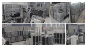
表1
Design of the New Production Line
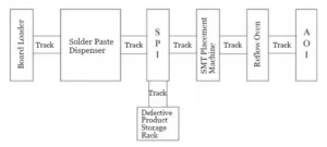
Engineers addressed the current issues with the PCB assembly prototype production line by using a solder paste dispensing machine to replace the solder paste printer in the SMT production line.
This change creates a new prototype production line design, as shown in Figure 3.
Core Equipment Configuration
The new production line primarily consists of a board loader, solder paste dispensing equipment, a solder paste inspection (SPI) machine, a scrap rack, a pick-and-place machine, a reflow oven, and an AOI machine.
The board loader places the PCB boards onto a conveyor track to transport them to subsequent processes, while the solder paste dispensing equipment calls up the corresponding program based on the PCB model to dispense solder paste.
Process Stability and Quality Control Considerations
A small amount of air in the dispensing cartridge can prevent solder paste from reaching the pads, resulting in poor soldering quality.
Improper maintenance of the dispensing cartridge can cause the solder paste at the nozzle outlet to dry out.
This condition reduces the dispensing volume or even blocks the nozzle completely, leading to insufficient or no solder paste and preventing components from being soldered.
Technicians install a scrap rack next to the SPI machine to stop defective products from entering subsequent processes, reducing the soldering defect rate.
After surface-mount placement, the system performs reflow soldering, followed by AOI inspection.
Manufacturing Efficiency and Flexibility Advantages
The new PCBA prototype SMT production line does not require the fabrication of stencils; solder paste is printed directly onto the PCB pads.
This eliminates the need for stencil cleaning, saving labor hours, reducing material waste, and making the process more eco-friendly.
Operators can switch between solder paste printing programs for different PCB models easily and conveniently.
This capability enables rapid production line changeovers. It also ensures high production efficiency and meets the demands of high-mix, low-volume production.
Manufacturers produce steel stencils only after validating the PCB prototype.
This approach reduces the number of stencils and lowers associated costs. It also conserves limited production storage space.
In addition, the method shortens the production cycle by at least two days.
High-Density, Fine-Pitch Component Applications
As PCB assembly (PCBA) designs evolve toward lighter, thinner, shorter, and smaller form factors, components continue to become increasingly miniaturized.
With the widespread adoption of fine-pitch PCB technology, component layouts on PCBs are becoming increasingly dense.
At the same time, ball grid array (BGA) packaging has also become widely used;
For certain specialized products, PCB surface-mount pads are designed with a recessed structure.
In response to these application requirements, the limitations of traditional solder paste printers have become increasingly apparent.
Micro-components and High-Density Layouts
Due to their small size and ease of soldering, surface-mount components have replaced through-hole components as the mainstream choice for PCBA assembly.
The quality of solder paste printing is critical to the soldering quality of surface-mount components.
Micro SMT components such as 01005 and 0201 have high requirements for solder paste formation quality.
Conventional stencil printing methods lack sufficient precision, resulting in poor solder paste formation that fails to meet these requirements.
This problem is especially pronounced when components are densely packed on a PCB. Stencil printing becomes more prone to defects in these cases.
Common defects include solder bridging, insufficient solder, solder balls, missed printing, and collapse.
PCB assemblies typically use multi-pin high-speed surface-mount connectors to establish signal control connections with other components, such as 180-pin high-speed surface-mount connector sockets.
These connectors feature a large number of densely packed pins with extremely small spacing, which exceeds the precision capabilities of conventional stencil printing, leading to widespread defects such as solder bridging, insufficient solder, and missed printing.
These defects result in a significant increase in post-soldering defect rates, severely impacting production quality and efficiency.
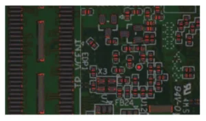
The process uses solder paste jetting equipment to apply high-precision solder paste onto PCB pads for micro-SMT components, such as 01005 and 0201, and 180-pin high-speed SMT terminal sockets.
Figure 4 shows the results of the localized jetting.
BGA-type Chip Components
BGA-type chip components feature a large number of densely packed solder joints and extremely small pad sizes.
Stencil printing cannot achieve the precision required for forming solder paste on high-density, fine-pitch pads.
Operators cannot precisely control the amount of solder paste on each pad.
These limitations often cause defects, such as insufficient solder and missed prints.
These defects are the primary causes of BGA soldering failures, severely impacting production quality and efficiency.
Case Study: 2024 Production Data
Taking our company’s 2024 data as an example, there were a cumulative total of 177 failures across several major BGA chip models, as shown in Table 2.
Technicians disassembled the BGAs using a rework station and cleaned them, then re-balled the BGAs using specialized fixtures.
After reflow soldering, the PCBs underwent secondary testing, which eliminated the BGA failures.
This further validated that solder paste defects caused by stencil printing were the root cause of the BGA chip failures.
表2
The disassembly and repair of BGA-type chips require not only specialized rework platforms but also personnel with specialized skills.
The process is difficult, time-consuming, and costly, which severely impacts production throughput.
Advantages of Solder Paste Dispensing
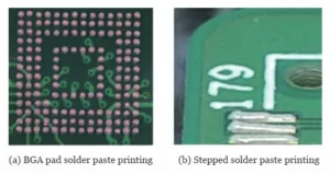
Solder paste dispensing equipment offers high dispensing accuracy, enabling not only high-precision formation but also the ability to adjust the solder paste volume based on the shape and size of different BGA chip pads.
It can also dispense solder paste in a stepped pattern, as shown in Figure 5.
The solder paste volume and shape are uniform across all identical pads on the BGA, ensuring consistent soldering at all joints.
Printing stepped solder paste meets the soldering requirements for surface-mount components with gull-wing leads. This process improves the reliability of lead soldering.
It also increases the strength of the solder joints that secure the BGA chip. As a result, the overall performance stability improves.
PCB Surface-Mount Pad Recess Layout
A PCB surface-mount pad recess layout improves soldering reliability, reduces impedance spikes in signal transmission paths, and enhances the connection strength between the pads and the copper traces.
PCBs with special requirements often adopt this design approach, featuring a high-density arrangement of surface-mount pad recesses on the PCB to enhance the overall stability of the product.
This structure stops the stencil from printing solder paste onto the pads within the recesses.
Traditional manual soldering is difficult, yields poor quality, and results in low production efficiency.
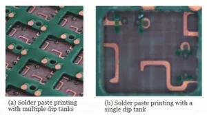
Solder paste dispensing equipment also handles PCB surface-mount pad recessed designs.
It solves the problem where stencil printing cannot accommodate height differences in the surface-mounted pads.
Solder paste inkjet equipment can rapidly and precisely apply solder paste to pads within recesses, resulting in excellent solder paste formation quality and high consistency, as shown in Figure 6.
Placing reference marks within the recesses can further enhance the precision of the solder paste inkjet application.
Design of PCB Assembly Mass Production Line Solutions
Analysis of Solder Paste Dispensing Equipment Production Efficiency
Currently, solder paste dispensing equipment can theoretically achieve speeds of over 1 million dots per hour (approximately 300 dots per second).
In actual production applications, the equipment maintains an average speed of 200 dots per second, demonstrating extremely high dispensing speeds.
Comparative Efficiency Analysis of Mass-Production PCB Models
By selecting three standard mass-production PCB models—S1, S2, and S3—for solder paste
printing, we analyze the actual production efficiency of the solder paste printing equipment and compare it with the current production efficiency of a company’s SMT production line.
The production efficiency of an SMT production line depends on the time it takes for a PCB to pass through the reflow oven; therefore, the time spent in the reflow oven is used as the reference benchmark, as shown in Table 3.
The production time for S2 and S3 solder paste printing is five times that of the reflow process on the SMT production line, while the production time for S1 double-sided solder paste printing is 2 times and 4.6 times that of the reflow process on the SMT production line, respectively.
表3
Prototype vs Mass Production Suitability
Solder paste jetting equipment operates with lower efficiency than reflow soldering.
However, the small number of PCB prototypes produced for each model makes this difference negligible.
Manufacturing matching SMT stencils requires a 2–3-day lead time, which outweighs the efficiency gap.
Therefore, solder paste jetting equipment can fully replace solder paste printers in PCB prototype production lines.
Unlike prototype production, the PCB assembly mass production stage involves larger production volumes.
Mass production lines operate on tight schedules and maintain fast production rhythms.
Solder paste spray equipment cannot match the efficiency requirements of these lines.
This mismatch reduces production efficiency, affects delivery times, and increases production costs.
Consequently, solder paste dispensing equipment does not yet meet the conditions to directly replace solder paste printers in PCBA mass production lines.
Design of a New Production Line for PCB Assembly Mass Production
Proposal 1 addresses the issue of solder paste dispensing equipment failing to match the production efficiency of the PCB assembly mass production line.
It also improves solder paste coverage on pads and enhances soldering quality.
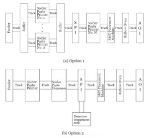
The proposal introduces a parallel production line design for solder paste dispensing equipment, as shown in Figure 7(a).
Solution 1 employs multiple solder paste dispensing machines operating in parallel to boost production efficiency.
Buffer and Secondary Dispensing Optimization
One buffer machine is installed before the parallel dispensing process, and another is installed after.
These machines increase PCB assembly throughput. The setup meets the production efficiency requirements of the mass production line.
It also effectively replaces the solder paste printer.
The process adds one solder paste dispensing unit after the SPI inspection. This unit performs secondary dispensing on pads with insufficient solder paste, improving solder joint quality.
Evaluation of Solution 1
Solution 1 offers advantages such as a high degree of integration, elimination of stencil fabrication, short production cycles, low production costs, high solder joint quality, and low rework rates.
However, since the current unit price of solder paste spraying equipment is approximately one million yuan, the production line construction costs for Solution 1 are very high, making it difficult to widely promote and apply.
Integrated Hybrid Production Line Concept (Solution 2)
We further propose Option 2—an integrated production line design combining the solder paste jetting equipment with the solder paste printer, as shown in Figure 7(b).
In Solution 2, a solder paste jetting device is added after the solder paste printing process in an existing PCBA mass production line.
Functional Division Between Printing and Jetting Systems
The solder paste printing machine handles the pads for standard components, while the solder paste jetting device is responsible for jetting solder paste onto the pads of components with difficult-to-print areas.
The solder paste spray printer and the solder paste printer complement each other perfectly, significantly reducing the performance requirements for the solder paste printer.
The production line in Solution 2 offers excellent compatibility, high production flexibility, superior soldering quality, and a low PCBA defect rate.
Design of a New Repair Process for PCB Assemblies
With the widespread adoption of high-density, fine-pitch components such as BGA chips, 0201 micro-components, and multi-pin high-speed connectors, the defect rate in PCBA production has increased accordingly, making it essential to enhance PCBA repair capabilities and quality.
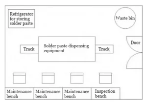
The new repair station should include at least one solder paste dispensing machine, a refrigerator for storing solder paste, a waste bin, an inspection station, and a repair station, as shown in Figure 8.
The repair station requires only one employee per shift to handle the repair, inspection, and storage of solder paste for components such as BGAs, resulting in low production costs.
The solder paste dispensing equipment enables high-precision dispensing onto component pads, reducing repair difficulty, ensuring high-quality solder joints, and improving the overall quality of PCBA repairs.
Conclusion
This paper aims to shorten the production cycle of PCBA prototypes.
It seeks to reduce production costs. The formation quality of solder paste on high-density, fine-pitch component pads improves significantly.
It enhances soldering quality. The paper also investigates the feasibility of applying solder paste inkjet equipment in PCBA production.
The paper analyzes the current issues in PCBA prototype production.
It proposes a new PCBA prototype production line solution that replaces traditional solder paste printers with solder paste inkjet equipment.
This solution shortens production cycles. It also provides high flexibility.
Researchers conducted an application study and analysis of solder paste inkjet technology for high-density, fine-pitch components.
This study successfully solved the problems caused by poor solder paste printing on the pads of these components.
The production efficiency of solder paste jetting equipment was then analyzed.
Based on the analysis, two new design schemes for PCBA mass production lines were proposed.
Considering production line construction costs, the integrated design that combines solder paste jetting equipment with a screen printer proved to be the most cost-effective solution.
Finally, the PCBA repair process was optimized to enhance repair efficiency and improve rework quality.
The research results indicate that adopting solder paste jetting technology shortens the production cycle for PCB assembly prototypes. It also reduces stencil procurement costs.
The technology improves the soldering quality of high-density, fine-pitch components. It increases the mass production yield rate of PCB assemblies.
Overall, it enhances the quality of the company’s PCB assembly products.

