
As a new type of stencil-free solder paste application technology, solder paste spray printing has demonstrated significant practical value in the production of military electronic products due to its convenience and flexibility.
Solder paste inkjet printing is a non-contact application method that offers the advantages of pressure-free operation, strong precision control, and high material utilization.
By selecting different printing parameters based on the pad size, it resolves coating quality issues associated with the mixed assembly of components with varying pad dimensions.
Currently, there is limited research on solder paste inkjet technology in China.
Peng Chen et al. have described the main structure and working principles of inkjet printers, while Zhu Yongxin et al. have studied reflow soldering techniques for inkjet-applied solder paste.
However, research on inkjet parameters for different packaged components remains incomplete.
Inkjet printing uses a coating method that differs from traditional stencil printing.
This difference leads to significant variations in solder joint morphology and makes inspection of the coating results difficult.
Applying SPI inspection standards designed for traditional stencil printing to inkjet-printed solder paste significantly increases false positive and false negative rates, and causes inspection results to deviate substantially from actual conditions.
Currently, manufacturers do not offer SPI devices specifically designed to inspect the quality of spray-applied solder paste.
Therefore, optimizing traditional SPI thresholds to accommodate this new spray-application technology has become particularly important.
Test Materials and Methods
Device Package Selection and PCB Design
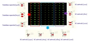
This test involves 10 types of RC components with different package types, as shown in Table 1. The PCB pad dimensions are shown in Figure 1.
Engineers use FR-4 as the PCB material with a thickness of 1.6 mm. The surface treatment applies leaded tin plating, and the design meets standard military-grade quality requirements.
| Component Name | Package Type |
|---|---|
| Resistor / Capacitor | 0402, 0603, 0805, 1206, 1210, 1812, 2220 |
| Tantalum Capacitor | 3528, 6032, 7343 |
Table 1. Component Package List
Design of Screen Printing Process Parameters
This study selects Sn63Pb37 solder paste, which contains metal particles with diameters ranging from 15 to 25 μm.
The screen printing equipment used in the experiments had a printing diameter range of 0.33 to 0.52 mm and a printing height of 1,000 μm.
| Test No. | Package Type | Preset Area Ratio / % | Preset Volume Ratio / % |
|---|---|---|---|
| 1 | 0402 | 100 | 60, 80, 100, 120, 140 |
| 2 | 0603 | 100 | 60, 80, 100, 120, 140 |
| 3 | 0805 | 100 | 60, 80, 100, 120, 140 |
| 4 | 1206 | 100 | 60, 80, 100, 120, 140 |
| 5 | 1210 | 100 | 60, 80, 100, 120, 140 |
| 6 | 1812 | 100 | 60, 80, 100, 120, 140 |
| 7 | 2220 | 100 | 60, 80, 100, 120, 140 |
| 8 | 3528 | 100 | 60, 80, 100, 120, 140 |
| 9 | 6032 | 100 | 60, 80, 100, 120, 140 |
| 10 | 7343 | 100 | 60, 80, 100, 120, 140 |
Table 2. Inkjet Printing Process Parameters
Test Results and Analysis
Calculation of the Equivalent Conversion Between Sprayed Solder Paste Volume and Printed Solder Paste Volume
A 0.12 mm thick stencil performed the solder paste printing process.
After printing, an SPI (Solder Paste Inspection) system inspected the solder paste deposit.
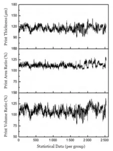
The system collected data from 2,500 solder paste samples, including thickness, area ratio (actual solder paste area / PCB pad area), and volume ratio [actual solder paste volume / (PCB pad area × 0.12 mm)].
The results are shown in Figure 2. Table 3 presents the mean, standard deviation, and coefficient of variation for the 2,500 sets of stencil printing data.
Analysis indicates that the stencil printing quality is highly consistent, with a mean printing thickness of 116.63 μm, a mean area ratio of 112.91%, and a mean volume ratio of 109.81%.
| Item | Mean Value | Standard Deviation | Coefficient of Variation |
|---|---|---|---|
| Print Thickness | 116.63 μm | 7.47 | 6% |
| Print Area Ratio | 112.91% | 4.65 | 4% |
| Print Volume Ratio | 109.81% | 9.14 | 8% |
Table 3. Mean and Standard Deviation of Print Quality
Solder Paste Material Characteristics
As a soldering material, solder paste plays a crucial role in soldering quality.
Manufacturers typically compose it as a uniform mixture of alloy solder powder and paste-form flux.
Basis for Inkjet and Screen Printing Comparison
To facilitate comparison of the amount of solder paste applied via inkjet printing and screen printing, this paper uses the volume ratio of solder paste as a reference.
According to Equation (1), the calculated theoretical solder paste volume ratio for inkjet printing is 114.91%.
Inkjet printing can achieve a solder paste volume ratio of 114.91%. This value corresponds to the volume ratio obtained through screen printing using a 0.12 mm stencil, and engineers treat the two as equivalent.
Theoretical Volume Ratio Calculation
VTheory = (Vreference × q₁) / q₂ (109.81% × 90%) / (86%) = 114.91% (1)
In the equation: Vref is the average volume fraction of solder paste in screen printing.
q₁ is the metal content ratio of the solder paste used for screen printing; q₂ is the metal content ratio of the solder paste used for inkjet printing.
Patterns of How Printing Process Parameters Affect Print Quality
Engineers applied the printing process parameters listed in Table 2 to print resistors and capacitors across 10 different package types.
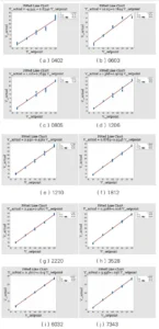
After printing, SPI collected data on the printed volume ratio and generated the fitting curve and formula shown in Figure 3.
The results show a linear relationship between the preset volume ratio and the actual volume ratio for resistor-capacitor devices.
Determination of Theoretical Preset Volume Ratio
Using the fitting formula, the analysis calculated the theoretical preset volume ratio corresponding to a theoretical solder paste volume ratio of 114.91%.
The calculation then rounded this theoretical preset volume ratio to obtain the actual preset volume ratio.
Subsequently, the team conducted printing tests using the actual preset volume ratio and measured the resulting actual volume ratios.
Comparison revealed that the mean of the actual volume ratios for some prints differed from 114.91%.
Iterative Adjustment and Optimization
The process adjusted the actual preset volume ratio to improve accuracy. Printing tests then repeated until the adjusted actual volume ratio approached 114.91%.
Table 4 presents the test results.
Preset Volume Ratio Settings for Different Components
| Component Name | Package Type | Reference Target Volume Ratio (%) | Theoretical Preset Volume Ratio (%) | Actual Preset Volume Ratio (%) | Actual Volume Ratio (%) | Adjusted Actual Preset Volume Ratio (%) | Adjusted Actual Volume Ratio (%) |
|---|---|---|---|---|---|---|---|
| Resistor / Capacitor | 0402 | 114.91 | 137.12 | 140 | 117.67 | 140 | 116.32 |
| Resistor / Capacitor | 0603 | 114.91 | 166.49 | 165 | 129.63 | 140 | 110.43 |
| Resistor / Capacitor | 0805 | 114.91 | 147.63 | 150 | 125.44 | 140 | 114.35 |
| Resistor / Capacitor | 1206 | 114.91 | 125.98 | 125 | 123.37 | 115 | 108.96 |
| Resistor / Capacitor | 1210 | 114.91 | 125.87 | 125 | 126.22 | 115 | 112.46 |
| Resistor / Capacitor | 1812 | 114.91 | 121.26 | 120 | 120.59 | 115 | 116.63 |
| Resistor / Capacitor | 2220 | 114.91 | 122.20 | 120 | 122.24 | 115 | 116.33 |
| Aluminum Electrolytic Capacitor | 3528 | 114.91 | 113.89 | 115 | 116.99 | 115 | 116.16 |
| Aluminum Electrolytic Capacitor | 6032 | 114.91 | 113.21 | 115 | 117.94 | 115 | 117.12 |
| Aluminum Electrolytic Capacitor | 7343 | 114.91 | 103.54 | 105 | 105.90 | 115 | 115.65 |
Table 4. Preset Volume Ratio Settings for Inkjet Printing of Different Packaged Components
SPI Thresholds for Solder Paste Dispensing
Engineers performed repeatability tests by adjusting the actual preset volume ratio (Table 4) to calculate the mean values and standard deviations of dispensed thickness, area ratio, and surface-to-volume ratio.
Table 5 presents the results. The data show that the mean thickness is approximately 150 μm, the mean area ratio is approximately 90%, and the mean volume ratio is approximately 115%.
Based on these results, the analysis determines the SPI inspection parameters for thickness, area ratio, and volume ratio as 150 μm, 90%, and 115%, respectively.
For SPI control limits, the method adopts ±3σ as the primary control boundary.
Factors Influencing SPI Threshold Establishment
In actual production, various factors such as temperature, humidity, solder paste type, solder paste viscosity, pad design, and PCB flatness influence the printed morphology of solder joints.
When establishing SPI thresholds, engineers must adjust the inspection threshold range based on actual product conditions and production experience, in addition to accounting for the standard deviation.
SPI Threshold Parameters for Different Package Types
Table 6 presents the SPI threshold parameters determined through comprehensive evaluation.
| Component Name | Package Type | Inkjet Thickness Mean (μm) | Std. Dev. | Actual Area Ratio Mean (%) | Std. Dev. | Actual Volume Ratio Mean (%) | Std. Dev. |
|---|---|---|---|---|---|---|---|
| Resistor / Capacitor | 0402 | 150.58 | 6.49 | 92.71 | 6.24 | 116.32 | 7.44 |
| Resistor / Capacitor | 0603 | 154.63 | 4.92 | 85.70 | 5.09 | 110.43 | 6.97 |
| Resistor / Capacitor | 0805 | 163.32 | 4.24 | 84.02 | 5.85 | 114.35 | 5.86 |
| Resistor / Capacitor | 1206 | 146.92 | 5.01 | 89.00 | 5.54 | 108.96 | 6.28 |
| Resistor / Capacitor | 1210 | 151.13 | 6.94 | 89.29 | 6.36 | 112.46 | 4.35 |
| Resistor / Capacitor | 1812 | 151.67 | 7.09 | 92.27 | 5.81 | 116.63 | 6.20 |
| Resistor / Capacitor | 2220 | 151.12 | 5.50 | 92.37 | 7.01 | 116.33 | 5.17 |
| Aluminum Electrolytic Capacitor | 3528 | 152.94 | 6.51 | 91.14 | 4.62 | 116.16 | 6.37 |
| Aluminum Electrolytic Capacitor | 6032 | 152.95 | 6.07 | 91.89 | 4.38 | 117.12 | 7.13 |
| Aluminum Electrolytic Capacitor | 7343 | 151.23 | 4.46 | 91.77 | 5.68 | 115.65 | 5.37 |
Tab 5. Mean Values and Standard Deviations of Inkjet Thickness, Area Ratio, and Volume Ratio for Different Packaged Components
| Component Name | Package Type | Thickness / μm | Area Ratio / % | Volume Ratio / % |
|---|---|---|---|---|
| Resistor/Capacitor | 0402 | 150 ± 50 | 90 ± 30 | 115 ± 30 |
| Resistor/Capacitor | 0603 | 150 ± 50 | 90 ± 30 | 115 ± 30 |
| Resistor/Capacitor | 0805 | 150 ± 50 | 90 ± 30 | 115 ± 30 |
| Resistor/Capacitor | 1206 | 150 ± 50 | 90 ± 30 | 115 ± 30 |
| Resistor/Capacitor | 1210 | 150 ± 50 | 90 ± 30 | 115 ± 30 |
| Resistor/Capacitor | 1812 | 150 ± 50 | 90 ± 30 | 115 ± 30 |
| Resistor/Capacitor | 2220 | 150 ± 50 | 90 ± 30 | 115 ± 30 |
| Aluminum Electrolytic Capacitor | 3528 | 150 ± 50 | 90 ± 30 | 115 ± 30 |
| Aluminum Electrolytic Capacitor | 6032 | 150 ± 50 | 90 ± 30 | 115 ± 30 |
| Aluminum Electrolytic Capacitor | 7343 | 150 ± 50 | 90 ± 30 | 115 ± 30 |
Tab 6. SPI Threshold Parameters for Different Package Types
Verification of Solder Joint Reliability via Dispensing
The process adjusted the actual preset volume ratio (Table 4) to perform dispensing.
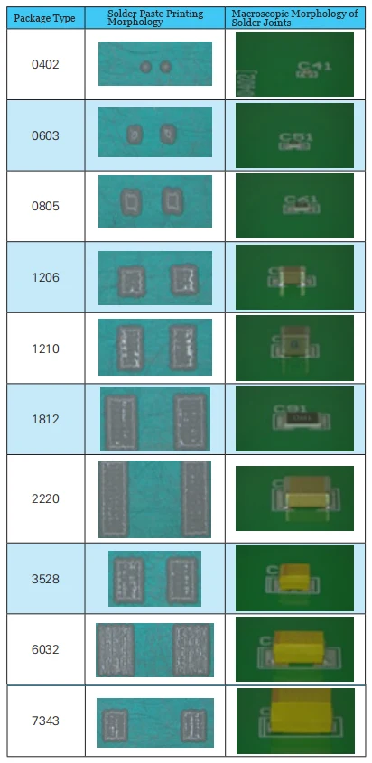
The results showed that the solder paste volume was appropriate and the thickness was uniform, with no instances of missed dispensing, over-dispensing, contamination, or splatter.
Microscopic inspection revealed that the solder joints had a full, rounded appearance, with a solder wick height exceeding 50%.
Inspection revealed no defects such as solder balls or solder dross, and the assembly met the requirements of the IPC-610 Class III standard.
Table 7 presents the validation results.
The solder joints were subjected to 200 temperature cycling tests to verify their adaptability in high- and low-temperature environments.
The temperature cycling test used a range from −50 °C to 100 °C.
The system controlled heating and cooling at a rate of 10 °C/min, and it maintained each extreme temperature for 15 minutes.
Each full cycle lasted 1 hour, and the test executed no fewer than 200 cycles in total.
Following temperature cycling, inspection of the solder joint appearance was conducted.
The evaluation indicated no abnormalities in the solder joints, and the entire board exhibited normal results.
Conclusion
This paper focuses on investigating the influence of preset volume ratios in solder paste printing on print quality.
Researchers established a method for determining SPI thresholds and obtained optimal printing process parameters and SPI thresholds for 10 types of packaged devices.
The experimental approach and methods described in the paper also extend their applicability to a wider range of packaged devices.
In future work, the author will conduct printing technology research on additional packaged devices to provide theoretical support for the application of printing technology in the defense industry.

