
As millimeter-wave radar technology finds increasingly widespread application in fields such as autonomous driving, aerospace, and security surveillance, the demand for high-performance printed circuit boards (PCBs) has grown accordingly.
Millimeter-wave radar relies on precise high-frequency signal transmission; therefore, the design and manufacturing quality of PCBs directly impact the functional performance of radar systems.
First, PCB layout is critical for signal transmission in millimeter-wave radar.
Improper layout can lead to signal reflection, crosstalk, and attenuation, thereby reducing the radar’s resolution and accuracy.
Second, material selection is also a key factor affecting millimeter-wave radar performance.
Traditional FR-4 substrates may not meet the requirements of high-frequency applications, necessitating the use of low-loss, high-performance substrates.
These materials provide better signal integrity and lower insertion loss, thereby enhancing the radar’s sensitivity and dynamic range.
Manufacturing Requirements
Furthermore, manufacturing processes significantly impact the functionality of millimeter-wave radar.
Precise control of PCB trace width and spacing, plating uniformity, and via hole accuracy are all critical to ensuring high-frequency signal transmission.
High-quality PCB manufacturing processes guarantee the accurate implementation of the design and prevent performance degradation caused by manufacturing defects.
Challenges
However, in the design of millimeter-wave radar antennas, compensation for rectangular right angles has always been a significant challenge.
Design specifications and technical parameter constraints limit compensation for inner and outer corners of rectangular angles.
Insufficient compensation causes beam inaccuracies and shifts in beam direction.
These deviations reduce detection accuracy and weaken target tracking performance in millimeter-wave radar systems.
Therefore, proposing an effective compensation scheme for the inner and outer corners of rectangular angles is crucial for improving the performance of millimeter-wave radar antennas.
Precision Control in PCB Fabrication
Engineers enhance the functional response of millimeter-wave radars through careful design.
Appropriate material selection improves overall system performance.
High-standard manufacturing processes further support high-performance radar requirements in modern electronic systems.
This paper examines right-angle etching precision in PCB fabrication for millimeter-wave radar antenna designs after applying rectangular right-angle compensation.
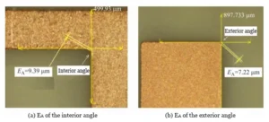
The study targets control of inner and outer corner tolerance (EA) within ≤15 μm, as shown in Figure 1.
Explanation of Manufacturing Challenges
(1) Right-Angle Etching Accuracy Challenges
Typical PCB manufacturing for 77 GHz millimeter-wave radar antennas produces rectangular right-angle features after etching.
Without applying characteristic compensation, these dimensions deviate significantly from customer design requirements.
For example, the inner angle EA of the rectangle is 43.24 μm, and the outer angle EA is 21.51 μm, neither of which meets the requirement of EA ≤ 15 μm.
(2) Characteristics of Millimeter-Wave Radar Antenna Boards:
① Surface copper thickness requirements are 10–20 μm, 21–30 μm, and 31–40 μm (customers generally require finished copper thickness to fall within these three ranges);
② Antenna line width tolerance requirements are ±10 μm, ±13 μm, and ±15 μm (customers generally require line width tolerances to fall within these three ranges);
③ The antenna line inner and outer corner (EA) requirements are EA ≤ 10 μm, EA ≤ 15 μm, and EA ≤ 20 μm (customers generally require the EA values for inner and outer corners to fall within these three ranges).
(3) Surface Copper Uniformity and Etching Requirements
To meet the antenna line width and inner/outer corner EA requirements, it is necessary to improve the uniformity of the surface copper plating and the etching capability:
① Surface copper plating uniformity requirements:
◆ VCP copper plating is used in the antenna area. The number of copper plating passes in the antenna area is ≤2, with a surface copper tolerance of ±3 μm. (If plating exceeds 2 passes, switch to a via plating process using via copper with a dry film mask to improve surface copper uniformity);
◆ If the customer requires an antenna line width tolerance of ±10 μm, the surface copper tolerance for the VCP-plated copper on the antenna layer (L1) is ±3 μm;
◆ If the customer requires an antenna line width tolerance of ±15 μm, the surface copper tolerance for the VCP-plated copper on the antenna layer (L1) is ±4 μm;
② Circuit processing: Process using a vacuum etcher.
③ Engineers apply compensation to the antenna line width and to both inner and outer corners of the line bends.
Process Specifications
Engineers apply a chemical tin-plating surface treatment to the antenna board.
They also classify the antenna-area copper thickness into three ranges: 10–20 μm, 21–30 μm, and 31–40 μm.
The primary objective is to verify the compensation for internal and external corners of the antenna lines at different copper thicknesses.
Outer Layer Process: (No resin-filled vias, stepped copper; finished copper thickness at antenna locations (25±5) μm, finished copper thickness in other areas (45±5) μm) Laminating → Outer layer vertical resin stripping → Outer layer resin grinding (no ceramic removal) → Copper reduction (14±1) μm → Laser drilling for windows → Laser drilling (0.2 mm) → Mechanical drilling → Plasma stripping → Horizontal copper plating → VCP via filling (surface copper (28±5) μm) → Outer layer dry film (covering antenna positions, positive film) → Outer layer pattern plating (copper plating without tin plating, surface copper (42±3) μm, aspect ratio 6.8:1, through-hole copper ≥20 μm, blind-hole copper ≥12 μm) → Dry film stripping → Outer layer dry film (negative side) → Outer layer acid etching → AOI → Solder mask → Hole inspection → Electrical testing → FQC (inspection) → Tinning → Normal process.
Results and Discussion
Compensation Design for the Inner and Outer Angles (EA) of the Antenna
The compensation design for this product differs from other compensation mechanisms; there is significant variation in the compensation shape and magnitude.
The process involves numerous tests, and the challenges in its implementation are as follows:
1. Design of the Compensation Shape for the Inner and Outer Corners of the Antenna
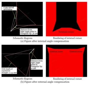
① The side length of the equilateral triangle used in the compensation shape design is 0.144 mm (significant changes to the side length will directly affect the right-angle shape).
② The antenna uses different compensation triangle shapes for inner and outer corners.
The inner corner experiences slower etching, while the outer corner undergoes faster etching.
These differences arise from variations in chemical solution exchange rates, as shown in Figure 2.
2. Design of Inner and Outer Corner Compensation for Antennas
(1) Engineers adjust inner and outer corner dimensions by shifting an equilateral triangle with a side length of 0.144 mm.
This adjustment maintains a constant distance between the triangle edges and the line width. CAM processing controls this relationship within a manufacturing tolerance of ±2.5 μm.
2) Engineers classify the antenna-area copper thickness into three ranges: 10–20 μm, 21–30 μm, and 31–40 μm.
Table 1 presents the corresponding rules for inner and outer corner compensation in antenna CAM fabrication.
| Copper Foil Thickness | Angle Position | Compensation Value |
|---|---|---|
| 31–40 μm | External Right Angle | Compensate the distance from the right-angle tip to the triangle tip by 46 μm |
| 31–40 μm | Internal Right Angle | Compensate the distance from the right-angle tip to the triangle tip by 41 μm + round the two crossing lines with an 8 μm radius |
| 21–30 μm | External Right Angle | Compensate the distance from the external right angle to the triangle tip by 41 μm |
| 21–30 μm | Internal Right Angle | Compensate the distance from the right-angle tip to the triangle tip by 36 μm + round the two crossing lines with a 6 μm radius |
| 10–20 μm | External Right Angle | Compensate the distance from the right angle to the triangle tip by 36 μm |
| 10–20 μm | Internal Right Angle | Compensate the distance from the right-angle tip to the triangle tip by 30 μm + round the two crossing lines with a 4 μm radius |
Table 1. Compensation Rules for Internal and External Angles in Radar Antenna CAM Fabrication
Test Results
Table 2 shows the test results for the inner and outer corner compensation rules of the antenna CAM, based on antenna surface copper thicknesses of 10–20 μm, 21–30 μm, and 31–40 μm.
The test results confirm that all cases satisfy the requirement of EA ≤ 15 μm.
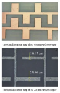
Table 2 and Figure 3 further show that inner corner machining presents greater difficulty compared with outer corner machining.
The process also produces lower EA values at the outer corners than at the inner corners.
As the copper thickness of the surface layer increases, the EA values for both the inner and outer corners of the antenna also increase (making machining more difficult).
With surface copper thickness at or below 40 μm and the proposed process applied, the inner and outer corner EA values of the antenna remain within specification and satisfy customer requirements.
When copper thickness exceeds 40 μm, manufacturing limitations increase EA values beyond the target range.
In this case, relaxing the inner and outer corner EA requirements is recommended (for example, allowing EA ≤ 20 μm or EA ≤ 25 μm).
| Copper Foil Thickness | Internal Angle EA (1) | Internal Angle EA (2) | External Angle EA (1) | External Angle EA (2) |
|---|---|---|---|---|
| 10–20 | 10.83 | 9.39 | 7.22 | 5.52 |
| 21–30 | 11.61 | 11.69 | 9.99 | 6.43 |
| 31–40 | 14.44 | 11.78 | 9.39 | 8.42 |
Table 2. Test Results of Internal and External Angle Compensation Rules
Conclusion
Careful design improves the accuracy of millimeter-wave radar systems.
Appropriate material selection supports stable electrical performance in antenna PCBs.
High-standard manufacturing processes further enhance signal integrity and overall radar precision.
This paper provides a detailed discussion of design solutions and compensation rules for internal and external corners on antenna boards, and offers feasible manufacturing strategies.

