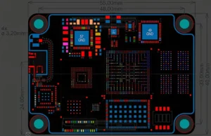
As PCB designs continue to evolve toward higher speeds, greater integration, and more compact form factors, trace routing has become one of the most critical factors affecting electrical performance, signal integrity, power stability, and electromagnetic compatibility (EMC).
Even when component selection and circuit design are optimized, poor routing practices can still lead to reflections, crosstalk, timing mismatches, excessive noise, and unexpected system failures.
To achieve reliable high-speed PCB performance, engineers must carefully consider every aspect of the routing process, including power distribution, trace geometry, spacing, impedance control, differential pair design, and length matching.
The following seven key routing considerations summarize the fundamental principles that help improve signal quality, reduce EMI risks, and ensure robust operation in modern electronic products.
PCB Power Supply Tracing
Digital circuits often require discontinuous current, which can cause inrush current in some high-speed components.
If the power supply traces are too long, the inrush current can generate high-frequency noise, which can then be introduced into other signals.
In high-speed circuits, parasitic inductance, resistance, and capacitance are inevitable. Consequently, this high-frequency noise will eventually couple into other circuits.
Furthermore, the presence of parasitic inductance reduces the maximum surge current a trace can withstand, leading to a voltage drop that may cause the circuit to fail.
Therefore, it is particularly important to place bypass capacitors in front of digital devices.
Since the energy transfer capacity of a capacitor is limited by the transmission rate, a combination of a large capacitor and a small capacitor is typically used to cover the entire frequency range.

Avoiding Hotspots: Signal vias can create voids in the power plane and ground plane.
Therefore, improper via placement can increase current density in certain areas of the power or ground plane. These areas of increased current density are referred to as hotspots.
Therefore, when placing vias, we must do our utmost to avoid this situation to prevent the planes from being fragmented, which could ultimately lead to EMC issues.
Typically, the best way to avoid hotspots is to place vias in a mesh pattern.
This ensures uniform current density, prevents the planes from becoming isolated, keeps return paths short, and thus avoids EMC problems.

PCB Trace Angles
When routing high-speed signal traces, bends should be avoided as much as possible. If a bend is unavoidable, avoid sharp or right angles; instead, use obtuse angles.

When routing high-speed signal lines, we often use serpentine routing to achieve equal lengths; however, serpentine routing is also a form of bending.
Line width, spacing, and bending methods should all be chosen appropriately, and spacing should comply with the 4W/1.5W rule.

Spacing Between High-Speed Signals on PCBs
If high-speed signal lines are too close together, crosstalk can easily occur. Sometimes, due to layout constraints or board dimensions, the spacing between high-speed signal lines may exceed the minimum required distance.
In such cases, we must maximize the spacing between high-speed signal lines as much as possible near the bottleneck areas.
In fact, if space permits, the spacing between two high-speed signal lines should be maximized as much as possible.

PCB Trace Stubs
A long stub acts like an antenna; if not handled properly, it can cause serious EMC issues. At the same time, stubs can also cause reflections, reducing signal integrity.
Stubs are most commonly generated when pull-up or pull-down resistors are added to high-speed signal lines; typically, stubs are managed by using daisy-chain routing.
Experience shows that if a stub is longer than 1/10 of a wavelength, it can be treated as an antenna, at which point it becomes a problem.

PCB Tracing: Impedance Discontinuities
The impedance of a trace generally depends on its width and the distance between the trace and the reference plane.
The wider the trace, the lower its impedance. The same principle applies to interface terminals and device pads.
Engineers often connect interface terminal pads to high-speed signal traces. A large terminal pad typically presents lower impedance, whereas a narrow high-speed trace exhibits higher impedance.
This difference creates an impedance discontinuity along the signal path.
As a result, the discontinuity may generate signal reflections and degrade signal integrity.
To mitigate this problem, designers typically remove copper directly beneath a large interface or component pad.
They then provide a reference plane for the pad on a different layer. This approach increases the pad impedance and helps maintain consistent impedance throughout the signal path.

Vias are another source of impedance discontinuities. To minimize this effect, unnecessary copper areas connecting the inner layers and vias should be removed.
This can be achieved during the design phase using CAD tools or by coordinating with the PCB manufacturer to eliminate unwanted copper areas, thereby ensuring impedance continuity.

High-Speed Differential Signals on PCBs
For high-speed differential signal lines, we must ensure equal width and spacing to achieve a specific differential impedance value.
Therefore, when routing differential signal lines, strive to maintain symmetry as much as possible.

Do not place vias or components within a differential pair.
Placing vias or components within a differential pair can cause EMC issues and result in impedance discontinuities.

Sometimes, high-speed differential signal lines require series coupling capacitors.
These coupling capacitors must also be placed symmetrically, and their packages should not be too large. 0402 and 0603 packages are recommended and acceptable; capacitors larger than 0805 or capacitors placed side-by-side should be avoided.

Typically, vias create significant impedance discontinuities; therefore, for high-speed differential signal pairs, minimize the use of vias as much as possible.
If vias must be used, arrange them symmetrically.

Equal Length of PCB Signal Lines
In some high-speed signal interfaces, such as buses, it is necessary to consider the arrival times and delay errors between individual signal lines.
For example, in a high-speed parallel bus, the arrival times of all data signal lines must be kept within a certain delay tolerance to ensure consistency in setup and hold times.
To meet this requirement, equal length must be ensured.
For high-speed differential signal pairs, strict delay matching between the two signal lines must be maintained; otherwise, communication failure is highly likely.
To meet this requirement, equal length can be achieved through serpentine routing, thereby satisfying the delay specifications.

Serpentine traces should generally be routed at the source of the length discrepancy, rather than at the far end.
Only at the source can we ensure that the signals on the positive and negative ends of the differential pair are transmitted in sync for the majority of the time.

Bends in the trace are one of the primary sources of length loss. To achieve equal length at a bend, the adjustment should be made close to the bend (≤15 mm).

If there are two bends in the trace and the distance between them is <15 mm, the length losses from both bends will compensate for each other; therefore, no additional equal-length adjustment is required in this case.

High-speed differential signal traces in different sections should be length-matched independently.
Via placements, series-connected coupling capacitors, and interface terminals can all split a high-speed differential signal trace into two sections, so special attention is required in these cases.
It is essential to ensure each section is length-matched separately. This is because many EDA software tools only check for overall length mismatch during DRC.

For interfaces such as LVDS display devices, multiple differential pairs may coexist, and the timing requirements between these pairs are generally very strict, with extremely small jitter tolerances.
Therefore, for such differential signal pairs, we generally require compensation to be performed within the same plane, as signal propagation speeds differ across layers.

Some EDA software includes traces inside pads in its length calculations.
If length compensation is applied in this scenario, the final result will actually result in a length discrepancy. Therefore, special attention must be paid when using certain EDA software.

Whenever possible, always choose symmetrical breakout to avoid having to use serpentine routing later to achieve equal lengths.

If space permits, try to add a small loop at the source of the short differential pair to achieve compensation, rather than using serpentine routing.

Conclusion
PCB routing is far more than simply connecting components.
It directly influences signal quality, power integrity, EMC performance, and overall system reliability.
Factors such as power supply routing, trace angles, signal spacing, stub control, impedance continuity, differential pair management, and length matching must all be evaluated together during the design process.
By following these seven routing principles, engineers can minimize signal degradation, reduce electromagnetic interference, improve timing consistency, and enhance product stability.
As data rates continue to increase and electronic systems become more complex, disciplined PCB routing practices remain essential for achieving successful high-speed designs and ensuring reliable long-term operation.