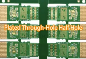
Half-hole (PTH half hole) PCB technology refers to a specialized plated through-hole structure formed by cutting standard through-holes along the edge of a printed circuit board, resulting in a semicircular or C-shaped plated contact.
Engineers widely use this design in modern electronics to enable direct board-to-board mounting of modules such as wireless communication boards onto main control boards.
By replacing traditional connectors and pin headers, half-hole structures help reduce assembly space, lower material costs, and support higher levels of integration.
Their applications span modular electronics design, compact device development, and certain testing or programming interfaces.
Definition of PTH Half Hole
PTH half hole is the abbreviation for Plated Through Hole half hole on a Printed Circuit Board (PCB).
We form it by cutting half of a plated through hole located at the edge of the PCB along the board edge, creating a semicircular or C-shaped hole with copper plating on its inner wall.


Design Purposes and Core Functions
Modular Board-to-Board Connection
This is the primary application of half-holes.
With half holes, we can directly surface-mount and solder PCB modules such as WiFi modules and Bluetooth modules onto main control boards just like IC chips.
The half holes on the side of the modules act as component pins, forming stable electrical connections with pads on the main board after soldering.
They can replace traditional pin headers and connectors, saving internal product space and reducing material costs.
High-Density Integrated Layout
Eliminating the space occupied by connectors helps miniaturize the overall product structure, which is especially suitable for portable electronic products with limited internal space.
Convenient Testing and Program Burning
In some designs, we use half holes as test points and programming interfaces.
We can test modules independently before assembling them onto the main board.
Typical Application Scenarios and Products
| Product Category | Typical Applications |
|---|---|
| Wireless Communication Modules | WiFi Modules (ESP Series), Bluetooth Modules, NB-IoT Modules, LoRa Modules |
| RF Modules | GPS Modules, GSM/GPRS Modules, RF Front-End Modules |
| Power Management Modules | DC-DC Power Modules, Battery Charging Management Modules |
| Sensor Modules | Various Intelligent Sensor Modules |
| Core Board / Computing Modules | Raspberry Pi Compute Module, Various ARM Core Boards |
| Storage Modules | eMMC Modules, SD Card Interface Modules |
Key Notes for Design, Production and Manufacturing
Layout Design Requirements
1. Distance from Hole Center to Board Edge
The dimension between the center of a half hole and the board edge needs precise control.
Conventional designs either align the hole edge flush with the board edge or leave a tiny clearance of 0.1–0.2 mm.
2. Pad Dimension Design
Pads matched for half holes shall be larger than those for ordinary plated through holes to ensure sufficient soldering area.
Designers should extend the pad outward beyond the board edge by 0.3–0.5 mm.
3. Hole Pitch Specification
The spacing between adjacent half holes must comply with SMT soldering process standards to avoid short circuits caused by solder bridging resulting from insufficient spacing.
Manufacturing Process Requirements
1. Sequence of Drilling and Routing
The manufacturing process proceeds with full-panel plating first, followed by contour routing via V-cut or routing machines.
The routing process tends to tear the copper foil on hole walls, so we require dedicated process control.
2. Electroplating Quality Requirements
After routing to form half holes, the copper plating on hole walls must remain intact without peeling or delamination.
3. Contour Machining Precision
The precision of CNC routing equipment directly determines the forming quality of half holes, so we must adopt high-precision routing machines in production.
For comprehensive design and manufacturing details of half-hole PCBs, you may refer to Several Considerations for Design and Fabrication of Half-Hole PCBs.
SMT Assembly and Soldering Requirements
1. Stencil Aperture Design
We must align stencil apertures precisely with half holes and strictly control the solder paste volume.
Excessive solder paste leads to short circuits, while insufficient solder paste causes cold solder joints.
2. Reflow Soldering Temperature Profile
Manufacturers must provide adequate heat for full wetting of solder paste when soldering half holes, and they must balance the temperature difference between modules and main boards.
3. Mechanical Structural Strength
Half holes provide lower bonding strength than complete plated through holes, so we must not use half-hole structures in positions subject to large external mechanical forces.
Long-term Reliability Requirements
1. Solderability Protection
Because we expose them at the board edge, half holes are prone to oxidation.
We recommend using surface finishes such as ENIG and OSP for protection.
2. Risks from Repeated Rework Soldering
Half-hole pads are prone to peeling during module rework, so we must reserve allowance for rework processes at the design stage.
Conclusion
Overall, half-hole PCB design plays an important role in achieving compact, high-density electronic assemblies while maintaining reliable electrical connections between modules.
However, its successful implementation depends heavily on precise layout design, strict manufacturing control, and careful SMT assembly processes.
Engineers must carefully manage factors such as edge distance, solder paste control, plating integrity, and rework limitations to ensure performance and long-term reliability.
When properly designed and manufactured, half-hole structures provide an efficient and space-saving solution for modern modular electronics.