
In modern PCB manufacturing, soldering processes play a critical role in ensuring the electrical performance, mechanical reliability, and production efficiency of electronic products.
Manufacturers widely use reflow soldering and wave soldering as the two primary assembly methods in SMT and THT production.
Although both processes achieve reliable solder joints, they differ significantly in application scenarios, component compatibility, PCB design requirements, and manufacturing processes.
Understanding the characteristics and selection principles of reflow soldering and wave soldering helps manufacturers optimize production processes.
It also improves soldering quality and enhances product reliability.
Reflow Soldering
Core Applications of Reflow Soldering
Surface-mount technology (SMT) uses reflow soldering as its core soldering process, and this process applies mainly to the following three categories:
1. Component Types
Surface-mount components include resistors and capacitors in 0402, 0603, 0805, and other packages.
They also include small surface-mount chips, such as QFP, QFN, and SOIC packages.
Other examples are ball grid array (BGA) and chip-scale package (CSP) components, as well as microconnectors, including FPC connectors and board-to-board connectors.
The common characteristics of these components are “no long leads, small size, and dense lead spacing.”
For example, BGA package pin pitch can be as low as 0.5 mm, and QFP pin pitch can reach 0.3 mm.
Traditional through-hole assembly processes cannot accommodate such components.
In contrast, reflow soldering, with its precise solder paste dispensing and uniform hot-air heating, ensures that each solder joint on densely packed pins forms uniformly.
It also prevents component damage caused by localized overheating.
Furthermore, for heat-sensitive components, such as sensors and RF chips, the gradual temperature curve of reflow soldering allows for precise control of the heating rate.
This reduces the risk of thermal damage.
2 PCB Design Requirements
Double-sided mounting PCBs, high-density routing PCBs (line width/spacing ≤ 0.1 mm), thin PCBs (thickness ≤ 1.0 mm), and multilayer PCBs (8 layers or more).
Reflow soldering of double-sided PCBs enables “simultaneous soldering on both sides” (or sequential soldering).
This eliminates the need for through-hole reservations and maximizes PCB area utilization.
High-density PCBs have extremely small pad spacings, where the solder wave in wave soldering can easily cause bridging.
In contrast, the solder paste printing accuracy of reflow soldering (up to ±0.05 mm) can prevent this issue.
Thin and multilayer PCBs are sensitive to thermal stress; the gentle heating curve of reflow soldering reduces the risk of board warping and internal layer solder joint failure.
In particular, the internal copper foil and substrate of multilayer PCBs have different coefficients of thermal expansion.
A gradual temperature ramp reduces the likelihood of delamination between layers.
3. Product Types
Consumer electronics include cell phones, tablets, and smartwatches.
Automotive electronics include in-vehicle navigation systems and sensor modules.
Medical electronics include portable diagnostic devices.
Telecommunications equipment includes routers and switches.
A common characteristic of these products is “miniaturization, high density, and high reliability.”
For example, the component density on a cell phone PCB can reach 1,000 components per square inch, making reflow soldering essential for achieving precise soldering;
Automotive electronics demand extremely high temperature stability.
The consistent solder joint performance of reflow soldering meets the requirements of operating environments ranging from -40°C to 125°C.
The typical surface-mount assembly process consists of three steps: the screen printer applies solder paste → the pick-and-place machine places the components → reflow soldering.
1. Applying Solder Paste with a Printing Machine
The purpose is to evenly apply the appropriate amount of solder paste to the pads on the PCB.
This ensures a good electrical connection between the surface-mount components and the corresponding pads on the PCB during reflow soldering.
Solder paste is a paste-like substance composed of alloy powder, paste-form flux, and additives, possessing a certain degree of viscosity and good wetting properties.
At room temperature, due to its viscosity, solder paste holds electronic components in place on the PCB pads;
Generally, components will not shift unless a significant tilt of the PCB or an external impact causes them to move.
When heat raises the solder paste to a certain temperature, the alloy powder melts and flows, and the liquid solder wets the component leads and PCB pads.
After cooling, the solder interconnects the component leads and pads, forming a solder joint that provides both electrical and mechanical connections.
2. Component Placement
This process involves using a placement machine or manual methods to accurately place surface-mount components onto the corresponding positions on the PCB surface.
Operators or manufacturers have pre-printed solder paste or adhesive onto the PCB surface.
There are two placement methods, compared as follows:
(1) Advantages and Disadvantages of Using a Placement Machine:
Machine printing, large batch sizes, tight delivery schedules, sufficient funding, high-volume production, high production efficiency, complex process, and significant investment!
(2) Manual placement:
Suitable for small to medium batch production and product R&D; simple operation; lower cost;
Production efficiency depends on the operator’s skill level.
Main tools for manual placement include: vacuum pick-and-place pens, tweezers, IC pick-and-place aligners, low-magnification stereomicroscopes, or magnifying glasses.
3. Reflow Soldering
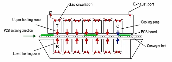
Reflow soldering process: First, when the PCB enters the preheating zone at 140°C to 160°C, the solvents and gases in the solder paste evaporate.
At the same time, the flux in the solder paste wets the pads, component terminals, and leads.
The solder paste softens and collapses, covering the pads and isolating them, along with the component leads, from oxygen.
This also ensures that the process thoroughly preheats surface-mount components.
Then, as the PCB enters the soldering zone, the temperature rises rapidly at a standard rate of 2–3°C per second, bringing the solder paste to a molten state.
The molten solder wets, diffuses, flows, and recirculates across the PCB pads, component terminals, and leads.
It mixes at the soldering interface to form metallic compounds and create solder joints.
Finally, the PCB enters the cooling zone, where the solder joints solidify.
Because the reflow soldering process features “re-flow” and “self-alignment effects,” it allows for relatively lenient requirements regarding placement accuracy.
This makes it easier to achieve a high degree of automation and high-speed soldering.
At the same time, precisely because of these re-flow and self-alignment effects, the reflow soldering process imposes stricter requirements on pad design and component standardization.
It also requires higher quality standards for component terminals, printed circuit boards, solder materials, and process parameter configuration.
Cleaning is the process of removing contaminants and impurities from the surface of an object through physical actions and chemical reactions.
Whether solvent-based or water-based cleaning is used, the process involves surface wetting, dissolution, emulsification, and saponification.
The cleaning process strips contaminants from the surface of the assembled board by applying mechanical force in various ways.
The operator then rinses or flushes the board to remove residues.
Finally, the operator air-dries, oven-dries, or naturally dries the board.
As a critical process in SMT production, proper temperature curve settings are key to ensuring the quality of the reflow soldering process.
An inappropriate temperature curve can lead to soldering defects on PCBs, such as incomplete soldering, cold joints, component lift-off, and excessive solder balls, which affect product quality.
Reflow soldering temperatures vary depending on the type of solder paste selected;
Leaded solder typically has a melting point of 180°, while lead-free solder generally has a melting point of around 210°.
Wave Soldering
Wave soldering is the dominant process for through-hole technology (THT). Its advantages lie primarily in the soldering of through-hole components, and it is suitable for the following applications:
1. Component Types
Through-hole components include DIP-packaged chips, through-hole resistors and capacitors, diodes, and transistors.
They also include high-power components, such as power modules, transformers, and inductors, as well as heavy-duty connectors, including pin headers and sockets, USB Type-C through-hole connectors, and power connectors.
These components feature “thick leads, rapid heat dissipation, and the ability to withstand mechanical stress.”
For example, the pin diameter of a power module can reach 1.0 mm, requiring sufficient solder fill and a high soldering temperature to form a secure joint.
The high-temperature solder wave (250–260°C) in wave soldering rapidly wets the pins.
The solder’s flowability ensures that the gap between the pin and the hole wall is completely filled, resulting in a joint with high tensile strength.
Heavy-duty connectors undergo frequent insertion and removal during use;
The “through-hole solder joints” formed by wave soldering provide stronger mechanical support, preventing pin loosening.
2. PCB Design Requirements
Single-sided through-hole PCBs, mixed-assembly PCBs (partially surface-mount + partially through-hole), thick PCBs (thickness ≥ 1.6 mm), and high-power PCBs (power boards, driver boards).
Hybrid assembly PCBs are a typical application scenario for wave soldering.
They typically employ a “reflow followed by wave” combined process.
First, manufacturers solder the surface-mount components using reflow soldering.
Then, manufacturers process the through-hole components using wave soldering.
At this stage, the surface-mount component areas need to be covered with high-temperature-resistant solder mask or protected with specialized carriers.
This prevents the solder joints from remelting due to secondary heating.
Thick and high-power PCBs dissipate heat rapidly.
The continuous heat from the tin wave in wave soldering ensures sufficient solder wetting.
In contrast, the hot air in reflow soldering struggles to penetrate thick boards and reach effective soldering temperatures.
Products such as power supply boards have large copper foil areas (which dissipate heat quickly);
The tin wave in wave soldering provides a more abundant heat supply, preventing “cold solder joints.”
3. Product Types
Industrial control equipment includes PLCs and variable frequency drives.
Power adapters are also common applications.
Security equipment includes surveillance cameras and network video recorders.
Home appliances include air conditioner control boards and washing machine drive boards.
These products have high requirements for mechanical strength and heat dissipation.
For example, the PCBs in industrial control equipment must withstand harsh environments such as vibration and shock;
In such cases, the vibration resistance of through-hole solder joints produced by wave soldering is superior to that of reflow soldering.
Additionally, the high-power components in power adapters require effective heat dissipation pathways;
Wave soldering provides a larger contact area between the solder joints and the copper foil, resulting in higher heat dissipation efficiency.
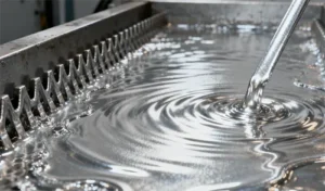
In wave soldering, a pump sprays molten solder into a wave.
The solder wave then passes over the leads of the electronic components to be soldered.
This establishes electrical connections between the components and the PCB.
4. Wave Soldering Process
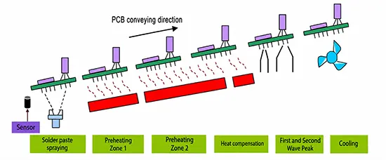
Insert components into the corresponding component holes → Pre-apply flux → Pre-bake (temperature 90–1000C, length 1–1.2m) → Wave soldering (220–2400C) → Trim excess component leads → Inspection.
The Difference Between Reflow Soldering and Wave Soldering
| Evaluation Criteria | Suitable for Reflow Soldering | Suitable for Wave Soldering | Suitable for Combined Process |
|---|---|---|---|
| Component Type | Pure SMD, fine-pitch leads, heat-sensitive components, miniature packages | Pure THT, high-power components, heavy connectors, thick leads | Mixed SMD + THT, with SMD components accounting for ≥50% |
| PCB Thickness | ≤ 1.0 mm | ≥ 1.6 mm | 1.0–1.6 mm, requires fixture support |
| Routing Density | Trace width/spacing ≤ 0.1 mm, pad spacing ≤ 0.3 mm | Trace width/spacing ≥ 0.2 mm, pad spacing ≥ 0.5 mm | Mixed-density layout; precision areas use reflow soldering |
| Target Industries | Consumer electronics, automotive electronics, medical electronics, telecommunications equipment | Industrial control, power adapters, household appliances, security equipment | Automotive electronics (high-power modules + precision sensors), industrial power supplies |
| Reliability Requirements | High-temperature stability, low corrosion risk, precision solder joints | High mechanical strength, enhanced heat dissipation, through-hole interconnection | Balances precision and mechanical strength; suitable for complex functional modules |
| Comparison Dimension | Reflow Soldering | Wave Soldering |
|---|---|---|
| Core Principle | Heated by hot air convection; solder paste is pre-printed and melts during reflow | Molten solder wave wets the PCB; liquid solder is supplied continuously in real time |
| Applicable Components | Surface Mount Devices (SMD): BGA, QFP, chip components, etc. | Through-Hole Technology (THT) components: DIP, high-power modules, connectors, etc. |
| Temperature Control | Four-stage precision temperature profile (Preheat → Soak → Reflow → Cooling); temperature accuracy of ±3°C | Stable solder wave temperature (250–260°C); preheating adjusted as required |
| Solder Supply | Solder paste is deposited in a controlled amount through stencil printing for precise solder joint size | Molten solder is supplied continuously, ensuring sufficient solder filling |
| Key Advantages | High precision, consistent solder joints, suitable for high-density assemblies, low thermal stress | High mechanical strength, good heat dissipation, ideal for through-hole components, relatively simple process |
| Typical Defects | Solder balls, cold solder joints, insufficient solder fillets (usually caused by improper solder paste printing) | Solder bridges, icicles, insufficient wetting / pin encapsulation (caused by improper wave height or conveyor speed) |
| Key Equipment Requirements | Multiple heating zones, uniform hot-air circulation, nitrogen atmosphere protection | Stable solder wave, dual-wave structure, precise conveyor system |
1. The reflow soldering process achieves mechanical and electrical connections between the leads of surface-mount components and the pads on the printed circuit board (PCB) by remelting the solder paste that manufacturers have pre-applied to the pads.
Wave soldering, on the other hand, involves melting a solder bar into a liquid state in a solder tank;
A motor then stirs the solder to create a wave, which is used to solder the PCB to the components.
This method is generally used for hand-inserted components and SMT boards with adhesive.
2. Wave soldering is suitable for hand-inserted boards and adhesive-coated boards, and requires that all components be heat-resistant;
Components that were previously soldered with SMT solder paste must not be present on the surface when passing through the wave.
Manufacturers can only process PCBs with SMT solder paste through reflow soldering and must not process them via wave soldering.
For double-sided SMT boards passing through the reflow oven, there are two processes: one uses solder paste on both sides, and the other uses solder paste on one side and red glue on the other.
Both processes follow a similar sequence: manufacturers populate and solder the first side first, then they process the second side.
Since the melting points of both solder paste and red glue after curing are higher than the temperature of the reflow oven, components will not fall off due to heat.
However, the side with solder paste cannot be re-processed via wave soldering, whereas the side with red glue can.
3. Wave soldering and reflow soldering processes differ: Wave soldering involves first spraying flux, followed by preheating, soldering, and then passing through the cooling zone.
Wave Soldering for Through-hole Components; Reflow Soldering for Surface-mount Components
In PCB manufacturing, the selection of reflow soldering versus wave soldering must follow a three-tier decision-making logic: “component type → PCB design → product reliability requirements.”
Only by precisely matching these factors to actual production scenarios can soldering yield and product stability be maximized.
The following are the specific selection steps and practical guidelines:
The packaging types and physical characteristics of components are the primary criteria for defining process boundaries.
It is necessary to first clarify the proportion and characteristics of the two types of components:
1. Pure Surface-Mount Device (SMD) Scenarios
If a PCB contains only surface-mount components such as SMDs, BGAs, and QFPs, with no through-hole leads, reflow soldering should be the preferred choice.
In particular, reflow soldering is the only suitable solution when components exhibit the following characteristics:
Lead pitch ≤ 0.5 mm (e.g., fine-pitch QFPs, micro BGAs);
Components are very small (packages smaller than 0402) or are heat-sensitive (operating temperature ≤ 150°C);
Components are of types with no exposed leads, such as ball grid arrays (BGAs) and chip-scale packages (CSPs).
2. Scenarios Involving Pure Through-Hole (THT) Components
If all components are through-hole type, high-power through-hole components, or heavy-duty connectors, wave soldering should be the preferred method.
The following characteristics further confirm the suitability of wave soldering:
Pin diameter ≥ 0.6 mm, and components subject to mechanical stress (such as interfaces requiring frequent insertion and removal, or components in vibrating environments);
Components with a heat dissipation capacity of ≥5 W (e.g., power modules, high-power inductors) that require enhanced heat dissipation via through-hole solder joints;
PCB designed as single-sided through-hole assembly with no surface-mount pads.
3. Mixed Assembly Scenarios (SMD and THT Coexistence)
This is the most common scenario in PCB production and requires a combined “reflow first, then wave soldering” process:
First, surface-mount components are soldered using reflow soldering to ensure the quality of solder joints on precision components;
Protect the areas containing surface-mount components (by applying high-temperature-resistant solder mask or using specialized fixtures) to prevent solder joints from remelting due to the high temperatures of wave soldering;
If the proportion of through-hole components is extremely low (≤5%), consider using “manual rework” as an alternative to wave soldering to reduce process complexity.
Conclusion
Reflow soldering and wave soldering each have their own advantages and suitable application areas.
Reflow soldering is mainly used for surface-mount components and high-density PCBs, offering precise control, high automation, and excellent soldering consistency.
Wave soldering is better suited for through-hole components, high-power devices, and applications requiring strong mechanical connections.
In practical PCB assembly, the choice between these two processes should be based on component types, PCB structure, and product reliability requirements.
By selecting the appropriate soldering method or combining both processes in mixed-assembly applications, manufacturers can achieve higher production efficiency, better soldering performance, and improved product quality.

