
Nowadays, whenever you open a PCB layout guide from an SoC manufacturer, it mentions the issue of corner angles for high-speed signal traces.
It always states that high-speed signals should not be routed at right angles but rather at 45-degree angles, and it often adds that routing in arcs is even better than 45-degree corners.
Is this actually the case? How should PCB trace angles be set—is a 45-degree angle better, or is routing in arcs better? Is routing at a 90-degree right angle actually acceptable?
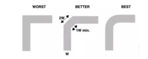
It’s only been in the last ten to twenty years or so that people have started worrying about the angles of PCB trace bends.
In the early 1990s, Intel, the dominant force in the PC industry, led the development of PCI bus technology.
(We owe a great deal of gratitude to Intel for introducing the PCI interface.
It was precisely the increased bandwidth provided by the PCI bus—and later the AGP bus—that gave rise to graphics cards like the 3DFX Voodoo.
Back then, we got our first taste of Lara Croft in *Tomb Raider*, as well as the exhilarating *Need for Speed 2* and the classic *Quake*, and more.
Looking back, it was precisely the market demand for 3D games and other multimedia applications that drove the advancement of PC technology.
This included the subsequent popularization of the internet and smartphones.
It seems that starting with the PCI interface, we entered an era of “high-speed” system design.
After the 1990s, it was precisely the thirst for 3D performance among a group of such gamers that enabled corresponding electronic design and chip manufacturing technologies to advance in line with Moore’s Law.
As IC manufacturing processes continued to improve, the switching speeds of IC transistors became faster and faster.
The clock frequencies of various buses also increased, and signal integrity issues attracted increasing research and attention.
For example, to meet today’s demand for 4K HD home entertainment video, the HDMI 2.0 transmission standard has already reached 18 Gbps!!!
Before I was born, PCB layout designers were probably relatively carefree.
They just needed to route the traces, keep them neat and tidy, and ensure a clean, aesthetic appearance.
They did not have to worry about various signal integrity issues.
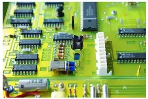
Take the circuit board of HP’s classic HP3456A six-and-a-half-digit multimeter, shown in the figure below, as an example: it features a large number of 90° angle traces.
The HP3456A has no “teardrops.”
The traces are almost deliberately routed at right angles.
In some places where a single angled trace would suffice, it uses several consecutive right angles instead.
The vast majority of the board lacks copper fill.
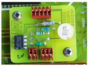
In the upper-right corner, not only does the line make a right angle, but the line width also gets thinner?
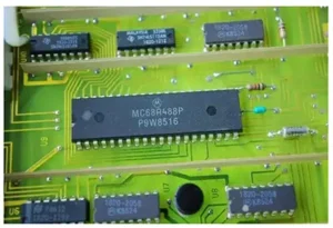
Right angles, bridging, and copper plating—is it really impossible to plate copper in a simulation?
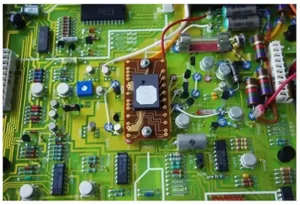
Right angles, 45-degree angles, arbitrary angles, square pads, round pads—but no teardrops.
Can a 90° bend in a high-speed signal line really cause a “pregnancy”? Is that how it works?
Here, Old Wu will use his own rudimentary approach to signal routing to discuss the issue of corner angles in high-frequency/high-speed signal routing with everyone.
We’ll look at routing from acute angles to right angles, obtuse angles, arcs, and all the way to arbitrary angles, examining the pros and cons of each corner angle.
Can PCB Traces Be Routed at Sharp Angles?
The answer is no. Setting aside whether routing traces at sharp angles would negatively impact high-speed signal transmission, from a PCB DFM perspective alone, sharp-angle traces should be avoided.
This is because where PCB traces intersect to form sharp angles, a problem known as “acid traps” can occur.
What? Pickled green beans? Well, I do like pickled green beans with noodles, but “acid traps” on a PCB are a real nuisance.
During the PCB manufacturing process, specifically during the etching stage, “acid traps” can cause excessive etching of the traces, leading to open circuits.
Although we can use CAM 350 to perform a DFF audit and automatically detect potential “acid trap” issues, this helps avoid manufacturing bottlenecks during PCB production.
However, if the PCB manufacturer’s process engineers detect an “acid trap,” they will simply patch the gap with a piece of copper.
Many PCB factory engineers actually lack a thorough understanding of layout; they merely address the “acid trap” issue from a PCB manufacturing perspective.
However, it remains unclear whether such a fix might lead to further signal integrity problems.
Therefore, we should strive to prevent “acid traps” from the very beginning during the layout phase.
How can we avoid creating sharp angles when routing traces that cause “acid trap” DFM issues?
Modern EDA design software (such as Cadence Allegro, Altium Designer, etc.) comes with comprehensive layout routing options.
By flexibly utilizing these auxiliary options during the layout process, we can greatly reduce the occurrence of “acid traps.”
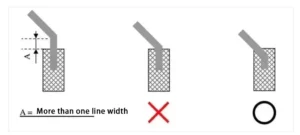
Set the pad exit angle to avoid sharp angles between the trace and the pad.
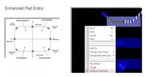
Using Cadence Allegro’s Enhanced Pad Entry feature allows us to avoid, as much as possible during layout, angles formed between traces and pads at the pad exit, thereby preventing “acid traps” as a DFM issue.
Avoid having two wires cross at an acute angle.
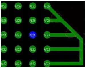
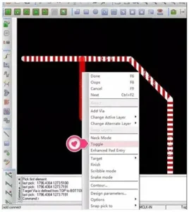
By flexibly using the “toggle” option in Cadence Allegro routing, you can prevent sharp angles from forming when routing wires into T-shaped branches, thereby avoiding “acid traps” as a DFM issue.
Can PCB Layout Use 90° Traces?
Why High-Speed PCB Signal Lines Should Avoid 90° Bends
High-frequency, high-speed signal transmission lines should avoid 90° bends—a requirement strongly emphasized in various PCB design guides.
This is because high-frequency, high-speed signal transmission lines need to maintain consistent characteristic impedance.
Using 90° bends alters the trace width at the bend.
The trace width at a 90° corner is approximately 1.414 times the normal trace width.
This change in width causes signal reflections, and the additional parasitic capacitance at the corner also introduces delay in signal transmission.
Of course, when a signal propagates along a uniform interconnect, it does not produce reflections or signal distortion.
However, if a 90° bend is introduced into a uniform interconnect, it will cause a change in the PCB trace width at the bend.
According to relevant electromagnetic theory, this will inevitably lead to signal reflections.
The Real Impact of 90° Corners on High-Speed and High-Frequency Signals
That’s the theory, but theory is just theory. In practice, is the impact of a 90° bend on high-speed signal transmission lines really that significant?
Let’s use an analogy. Say a student named Wang Shicong (this character is purely fictional for the sake of the story—surely no real father would name his son that, right?
Any resemblance to real people is purely coincidental, takes his family’s Siberian Husky and his girlfriend out for hot pot.
They spot a 100-yuan bill lying on the side of the road. Do you think he’ll pick it up or not?
Picking up that 100 yuan would, in theory, increase Wang Shicong’s personal wealth by 100 yuan.
But for Wang—who casually hooks up with girlfriends, has sex, and swipes his credit card to buy luxury cars as if they were cabbages—it’s completely negligible.
For me, though, that’s a fortune! I’d usually rush over and pretend to tie my shoelaces…
So, 90° corners do hurt high-speed signal transmission lines—theoretically, that’s for sure—but is this impact fatal?
Do 90° corners affect high-speed digital signal transmission lines and high-frequency microwave signal transmission lines in the same way?
Based on this paper, “Right Angle Corners on Printed Circuit Board Traces: Time and Frequency Domain Analysis,” Howard Johnson’s article “Who’s Afraid of the Big Bad Bend?,” and Chapter 8 of Eric Bogatin’s book *Signal Integrity and Power Integrity Analysis (2nd Edition)*, we can draw the following conclusions:
For high-speed digital signals, 90° corners do have a certain impact on high-speed signal transmission lines.
For today’s high-density, high-speed PCBs, where trace widths are typically 4–5 mil, the capacitance of a single 90° corner is approximately 10 fF.
Calculations show that the cumulative delay caused by this capacitance is approximately 0.25 ps.
Therefore, a 90° bend in a 5-mil-wide trace does not significantly affect current high-speed digital signals (with a 100-ps rise time).
However, for high-frequency signal transmission lines, wider traces are typically used to avoid signal degradation caused by the skin effect.
For example, a 50-Ω impedance trace with a width of 100 mils would have a trace width of approximately 141 mils at a 90° bend, resulting in a signal delay of about 25 ps due to parasitic capacitance.
In this case, the 90° bend would have a very severe impact.
At the same time, microwave transmission lines always aim to minimize signal loss as much as possible.
Impedance discontinuities at 90° corners and external parasitic capacitance can cause phase and amplitude errors in high-frequency signals.
They can also result in input-output mismatches and potential parasitic coupling.
These effects can degrade circuit performance and affect the transmission characteristics of PCB signals.
Modern PCB Routing Practices: Replacing 90° Corners with Better Layout Methods
Regarding 90° signal routing, Old Wu’s personal view is to avoid 90° bends as much as possible.
Wait, what? Didn’t we just say that the impact of 90° bends on high-speed digital signals is negligible?
Of course, what I wrote earlier was just to pad out the word count.
The impact of a single 90° corner on the signal quality of a high-speed digital transmission line is far less significant than other factors.
These factors include deviations in the height between the trace and the reference plane, variations in trace width and spacing uniformity during the etching process, changes in the board’s dielectric constant at different frequencies, and even the effects of via parasitic parameters.
However, in today’s high-speed digital circuits, transmission lines inevitably have to make equal-length bends.
When a dozen or two of these 90° bends are stacked together, the cumulative effect of these bends—resulting in signal rise time delays—becomes significant.
High-speed signals always travel along paths of least impedance; when routing around equal-length 90° bends, the final actual signal path ends up being slightly shorter than the original.
Furthermore, the transmission rates of high-speed digital signals are constantly increasing.
The current HDMI 2.0 standard already achieves a bandwidth of 18 Gbps, making 90° bends no longer acceptable.
Moreover, in the 21st century, modern EDA software—even the more basic versions—already provides excellent support for 45° bends.
At the same time, from an engineering aesthetics perspective, routing with 90° bends does not align well with people’s aesthetic sensibilities.
Therefore, in modern layout design—regardless of whether you’re routing high-frequency or high-speed signals—we should avoid 90° corners whenever possible, unless there are specific requirements.
For high-current traces, we sometimes use copper pads to replace the actual traces.
At the corners of these copper pads, 90° corners should also be replaced with two 45° corners.
This not only looks better but also eliminates potential EMI issues.
45° Tracing
Except for RF signals and other signals with special requirements, 45° tracing should be the preferred choice for traces on our PCBs.
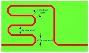
It is important to note that when routing 45° traces to ensure equal length, the trace length at the corner must be at least 1.5 times the trace width.
The spacing between traces routed to equal length must also be at least 4 times the trace width.
Since high-speed signals always travel along the path of least impedance, traces routed to equal length should not be placed too close together.
If the spacing between the traces is too small, the high-speed signal may take a shortcut due to parasitic capacitance between the traces.
This can result in inaccuracies in the equal-length routing.
Modern EDA software allows for the convenient configuration of relevant routing rules.
Using Curved Traces
Unless technical specifications explicitly require curved traces or the design involves RF microwave transmission lines, I personally don’t think it’s necessary to use curved traces.
In high-speed, high-density PCB layouts, a large number of curved traces are very difficult to edit later on, and they also take up a lot of space.
However, for high-speed differential signals such as USB 3.1 or HDMI 2.0, I believe it is acceptable to use curved traces.
Routing at Any Angle
The Impact of Increasing Signal Speeds on PCB Impedance and Signal Integrity
With the development of 4G/5G wireless communication technologies and the continuous upgrading of electronic products, PCB data interface transmission rates have now reached 10 Gbps or 25 Gbps and above.
Signal transmission speeds continue to increase.
As signal transmission becomes faster and operates at higher frequencies, stricter requirements are placed on PCB impedance control and signal integrity.
For digital signals transmitted on PCBs, many dielectric materials used in the electronics industry—including FR4—have traditionally been considered homogeneous during low-speed, low-frequency transmission.
However, when the electronic signal rate on the system bus reaches the Gbps level, this assumption of homogeneity no longer holds.
Glass Fiber Weave Effect and Its Influence on High-Speed PCB Signals
At this point, local variations in the relative permittivity of the dielectric layer caused by gaps between the glass fiber bundles interwoven in the epoxy resin substrate become significant.
These local perturbations in permittivity make the line’s delay and characteristic impedance spatially dependent, thereby affecting the transmission of high-speed signals.
Test data based on FR4 test boards indicate that differences in the relative positions of microstrip lines and glass fiber bundles cause significant fluctuations in the measured effective permittivity of transmission lines.
The difference in εr values can reach as high as △εr = 0.4.
Although these spatial perturbations may appear small, they can severely affect differential transmission lines operating at data rates of 5–10 Gbps.
PCB Layout Optimization and Future Trends in High-Speed Design
In some high-speed design projects, to mitigate the impact of the glass fiber effect on high-speed signals, we can employ zig-zag routing techniques to reduce the influence of this effect.
Cadence Allegro PCB Editor 16.6-2015 and later versions introduce support for zig-zag routing modes.
To enable the zig-zag routing feature, select “Route → Unsupported Prototype → Fiber Weave Effect” from the menu in Cadence Allegro PCB Editor 16.6-2015.
Time is a ruthless force—just as twenty years ago, we didn’t have to worry about whether to use curved traces in PCB layouts or about the impact of glass fiber in PCB substrates on high-speed signals.
Perhaps twenty years from now, when you read this again, you’ll find the views expressed here to be quite outdated…
Therefore, there are no immutable rules for PCB layout. As PCB manufacturing processes advance and data transmission rates increase, rules that are correct today may become obsolete in the future.
So, to be a qualified PCB router, you must keep pace with the times and stay abreast of the industry’s technological trends—only then can you avoid being weeded out by the tides of change.

