
When hardware engineers first encounter multilayer PCBs, they often find them confusing.
With as many as eight or ten layers, the traces look like a spider web.
I’ve drawn several diagrams of the internal structures of multilayer PCBs, using 3D models to illustrate the internal architecture of PCBs with various layer configurations.
Core of High-Density Interconnect (HDI) Boards Lies in the Via
The manufacturing process for multilayer PCBs is essentially the same as for single-layer and double-layer boards; the biggest difference lies in the via fabrication process.
The circuit patterns are etched, while vias are created by drilling holes and then plating them with copper—something everyone involved in hardware development already understands, so I won’t go into detail here.
Multilayer circuit boards typically include through-hole boards, first-order boards, second-order boards, and second-order stacked-via boards.
Higher-order types, such as third-order boards and arbitrary-layer interconnect boards, are rarely used in practice and are extremely expensive, so I won’t discuss them further here.
Generally, 8-bit microcontroller products use 2-layer through-hole boards;
Smart hardware at the 32-bit microcontroller level uses 4- to 6-layer through-hole boards;
Smart hardware running Linux or Android uses 6-layer through-hole to 8-layer first-order HDI boards; and compact products like smartphones generally use 8-layer first-order to 10-layer second-order circuit boards.
Most Common Through-Holes
There is only one type of via that extends from the first layer to the last.
Whether the traces are external or internal, the holes go all the way through; this is called a through-hole board.
Through-hole boards are not limited by the number of layers.
The 2-layer boards commonly used are through-hole boards, and many switchboards and military circuit boards, even those with 20 layers, are still through-hole boards.
A drill bit is used to drill through the circuit board, and then copper is plated inside the holes to form electrical pathways.
It’s important to note that the inner diameter of through-holes typically comes in 0.2 mm, 0.25 mm, and 0.3 mm sizes, but 0.2 mm holes are generally significantly more expensive than 0.3 mm ones.
This is because the drill bits are so fine that they’re prone to breaking, and the drilling process is slower.
The additional time and cost of the drill bits are reflected in the higher price of the circuit board.
Laser-Drilled Holes in High-Density Board (HDI Board)
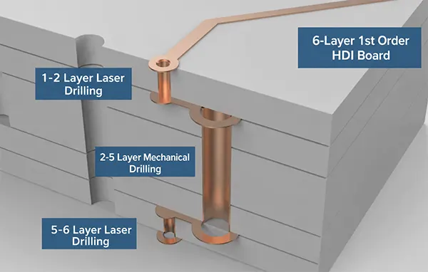
This diagram shows the layer stack-up of a 6-layer, Class 1 HDI board.
The two outer layers feature laser-drilled holes with an inner diameter of 0.1 mm.
The inner layers consist of mechanically drilled holes, equivalent to a 4-layer through-hole board, with two additional layers covering the outer surfaces.
Lasers can only penetrate glass-fiber-reinforced laminate; they cannot penetrate the copper.
Therefore, drilling holes on the outer surfaces does not affect the internal circuits.
After the holes are laser-drilled, the areas are plated with copper to form laser vias.
2-layer HDI Loard with Two Layers
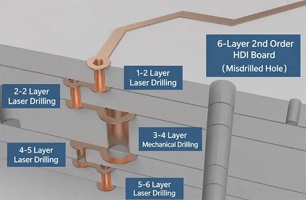
The image above shows a 6-layer, 2-stage staggered-hole HDI board. People rarely use 6-layer, 2-stage boards;
Most start with 8-layer, 2-stage boards. The same principle applies here, even with more layers.
“Second-order” refers to having two layers of laser-drilled holes.
“Offset holes” means that the two layers of laser-drilled holes are offset from each other. Why are they offset?
Because the copper plating does not completely fill the holes—there are voids inside—so additional holes cannot be drilled directly on top of them.
Instead, a certain distance must be left between the layers to create another layer of voids.
A 6-layer second-order board consists of 4 layers of first-order holes with an additional 2 layers on the outside.
An 8-layer second-order board consists of 6 layers of first-order holes with an additional 2 layers on the outside.
Stacked Perforated Plates: More Complex Manufacturing Process, Higher Price
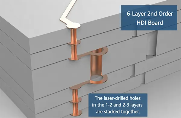
The two layers of laser-drilled holes on a staggered-hole board overlap. This results in a more compact layout.
The inner layer of laser-drilled holes must be filled via electroplating before the outer layer is drilled.
This process is slightly more expensive than the staggered-hole method.
Extremely Expensive Interlayer Interconnect Boards: Multi-Layer Laser-Stacked Vias
Every layer has laser-drilled holes, and every layer can be interconnected.
You can route the traces however you want and drill holes however you want.
Layout engineers get a real kick out of just thinking about it! No more worries about not being able to design a circuit!
Purchasing managers want to cry just thinking about it—it’s more than 10 times more expensive than a standard through-hole board!
That’s why only products like the iPhone can afford to use it.
As for other smartphone brands, I haven’t heard of any that have used multi-layer interconnect boards.
Conclusion
Understanding multilayer PCB via technology is essential for making informed design and sourcing decisions.
The progression from through-hole boards to first-order HDI, second-order stacked vias, and ultimately arbitrary-layer interconnects offers a clear tradeoff: each step upward delivers greater routing density and design flexibility, but at a dramatically higher manufacturing cost.
By matching the right board type to your product’s complexity level—whether it’s a simple 2-layer board for an 8-bit MCU or a 10-layer second-order HDI board for a smartphone—you can optimize both performance and budget in your next hardware project.

