
High-performance printed circuit boards are essentially precision multi-layer structures within electronic devices.
If the interlayer bonding fails, it can cause delamination and board failure, resulting in signal transmission abnormalities or distortion at best, and rendering the entire circuit board unusable at worst.
What is PCB Delamination?
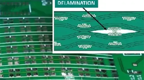
Delamination is a phenomenon in which the laminate material within a PCB separates between layers due to factors such as stress, temperature, and manufacturing processes.
The defect often causes blistering, cracking, or even fracturing of the board.
This issue not only significantly compromises the stability of circuit operation but also poses serious safety hazards, such as short circuits and fires.
Culprit Behind Delamination
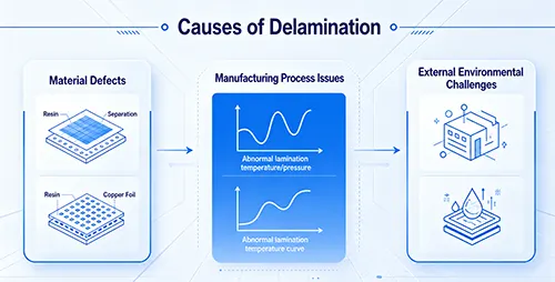
Material Defects
1. Moisture Absorption and Swelling of the P-Film or Substrate
The P-film and substrate have strict requirements for storage conditions:
Operators must keep the storage temperature at 20°C to 25°C and control relative humidity within 40%–60%.
If the storage environment does not meet these standards, the materials will gradually degrade in performance due to exposure to moisture and oxygen, ultimately leading to delamination and board failure.
2. Insufficient Bond Strength Between Copper Foil and Resin
Prior to the lamination process, defects in the browning treatment, insufficient surface roughness, and contamination on the copper foil surface can all weaken the bond strength between the substrate and the copper foil.
3. Mismatched Process Parameters (Temperature/Pressure/Time)
Excessively rapid heating can cause uneven expansion rates among the various materials in the PCB’s inner layers, increasing the risk of delamination;
Insufficient lamination time prevents the resin from fully curing, which also makes delamination defects more likely to occur.
Processing Issues
1. Drilling or Milling Parameters Mismatched with the Base Material
Excessively high drilling feed rates and operating speeds can exacerbate mechanical stress, causing stress concentration around the hole walls, which in turn leads to delamination between the resin, copper foil, and glass fiber cloth.
2. Residual Copper Plating / Electroplating Solutions
Operators must thoroughly rinse off residual chemicals left by copper plating and electroplating processes, these residues will keep corroding the inner copper foil;
Under certain conditions, alkaline substances that precipitate may also corrode organic substrates such as glass fiber and resin.
3. Differences in Thermal Expansion During High-Temperature Soldering
During high-temperature soldering, differences in the coefficients of thermal expansion between the copper foil and the glass fiber-resin substrate can lead to delamination when internal stresses exceed the material’s bonding limit.
External Environmental Challenges
1. Prolonged Exposure to High Temperatures and High Humidity
Long-term high-temperature and high-humidity harsh working conditions make the resin-based organic materials absorb moisture, which reduces their bonding strength with copper foil and fiberglass cloth.
2. Frequent Thermal Cycling
Frequent alternation between hot and cold temperatures gradually degrades the performance of PCB materials.
As the resin undergoes repeated thermal expansion and contraction, its molecular chains gradually break, leading to a decline in bonding strength.
How to Prevent Delamination and Board Rupture?
Material Control
Select high-quality, stable copper-clad laminates to ensure thorough impregnation of the glass fiber cloth and uniform resin distribution.
Strictly control storage temperature and humidity, maintaining a temperature range of 20°C–25°C and humidity of 40%–60% to prevent moisture absorption and damage to the boards.
Optimizing Manufacturing Processes
Adjust drilling speeds appropriately based on the board’s characteristics, and fine-tune lamination parameters—including temperature, pressure, and duration—in accordance with product specifications.
Design for Environmental Adaptability
Incorporate non-conductive heat dissipation holes to enhance the overall heat dissipation of the device;
Prioritize immersion gold surface treatment processes to improve the board’s resistance to damp heat.
Comprehensive Quality Control
Routinely monitor processes such as browning treatment and lamination temperature profile curves to ensure stable process operation.
Relying on incoming material inspections, semi-finished product cross-section inspections, and sampling verification of reflow-soldered products before shipment, we achieve comprehensive quality control throughout the entire production process.
How to Detect Delamination?
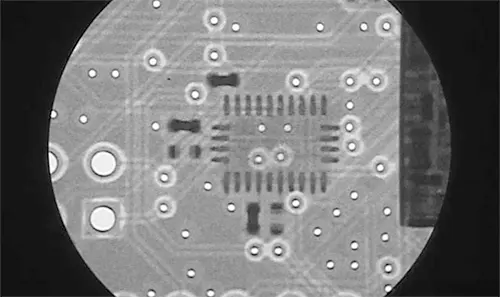
X-Ray Inspection
X-rays have extremely high penetrating power and can pass through all types of materials and internal structures in PCBs.
Different materials absorb and attenuate X-rays to varying degrees;
The higher the atomic number and density, the more significant the absorption.
Delaminated areas show distinctly different imaging features compared with intact areas, and technicians use X-ray scanning to detect defects like interlayer voids and cracks.
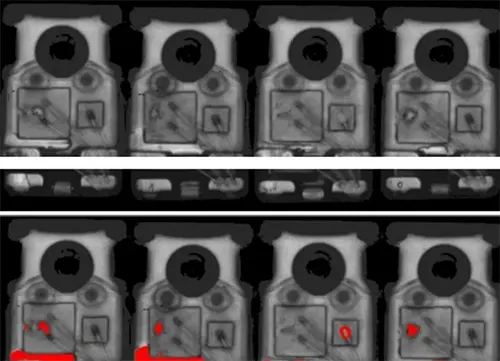
Ultrasonic Scanning Microscope (SAT)
The sound waves from the ultrasonic scanning microscope hit various internal interface boundaries of the PCB.
Material acoustic impedance differences reflect part of these waves, and the rest keep propagating inward.
Researchers can determine the exact location and size of delamination defects by analyzing high-frequency reflection signals.
Thermal Stress Testing (TST)
We subject the circuit board to repeated thermal cycling within a variable environment to simulate temperature changes under real working conditions.
Latent delamination issues within the board will gradually worsen under sustained thermal stress and may lead to other failures, thereby rapidly exposing delamination defects.
Cross-Section Analysis
Researchers cut a sample from the suspected delamination region. After embedding, grinding, and polishing it to form a flat, smooth cross-section, they visually inspect interlayer adhesion under a microscope.
Conclusion
PCB delamination is one of the most critical reliability issues affecting multilayer printed circuit boards.
Although it often begins as a microscopic separation between conductive and dielectric layers, it can quickly develop into blistering, cracking, open circuits, signal degradation, or complete board failure when exposed to mechanical stress or thermal cycling.
Preventing delamination requires a comprehensive approach that spans the entire PCB manufacturing lifecycle.
Manufacturers must select high-quality laminate materials, control storage temperature and humidity, optimize lamination and drilling parameters, thoroughly remove chemical residues, and implement rigorous quality control throughout production.
In addition, designing PCBs for the intended operating environment helps minimize stress caused by temperature fluctuations and moisture exposure.
Equally important is early defect detection.
Advanced inspection methods—including X-ray inspection, ultrasonic scanning, acoustic tomography (SAT), thermal stress testing, and cross-section analysis—allow manufacturers to identify hidden interlayer defects before products reach the field.
By combining proper material selection, robust process control, environmental design considerations, and comprehensive non-destructive testing, manufacturers can significantly reduce the risk of PCB delamination, improve long-term reliability, and ensure consistent performance in demanding electronic applications.

