
Printed circuit boards (PCBs) serve as the fundamental platform for component integration and signal transmission in electronic products and are widely used in consumer electronics, automotive, medical, and aerospace sectors.
According to statistics from an industry laboratory, cases of board-level failures caused by PCB defects account for more than 50% of all such failures.
In the electronics manufacturing industry, establishing a systematic quality management system and implementing end-to-end quality control can effectively reduce PCB failure rates, which is key to ensuring the stability of electronic products, the quality of complete systems, and improving economic efficiency.
Major PCB Failure Modes
Currently, typical failure modes for PCB products include short circuits, poor solderability, delamination, insulation failure, burnout, and poor bonding, among others.
According to failure data statistics from an industry laboratory, the top four failure modes attributable to the PCB itself are, in order:
Electrical failure (26.6%), poor solderability (22.3%), delamination (17.5%), and insulation failure (15.3%), which together account for 81.7% of all failures.
It is evident that these four categories—conductivity failure, poor solderability, delamination, and insulation failure—are the primary failure modes for PCB products.
Conductivity Failure
Conductivity failure primarily manifests as open circuits in traces, open vias, and failures in inner-layer interconnects.
1. Open Circuits
Both circuit defects and cracks can cause open circuits.
Circuit defects primarily stem from process issues during circuit formation, such as poor exposure (foreign objects or stains), the adhesion of anti-plating residues (e.g., dry film fragments, residual adhesive) to the copper surface during electroplating, over-etching during the etching process leading to localized circuit loss, and open circuits caused by scratches on the circuit during processing.
Circuit cracks typically occur during use.
For example, when a flexible printed circuit board (FPC) has kinks or scratches, fatigue fractures may occur after prolonged bending or vibration.
Additionally, mismatched thermal expansion coefficients of materials can cause the PCB to delaminate and crack under thermal stress, leading to conductor breaks.
2. Open Circuits in Holes
Open circuits can occur in through-holes, blind holes, and buried holes.
Abnormal copper crystallization in the holes is a common cause of hole wall fractures leading to open circuits.
Under normal conditions, the copper layer’s crystals should exhibit a dense, polyhedral block-like morphology with no obvious directionality in the crystal lattice arrangement, resulting in good ductility and tensile strength of the copper plating;
In contrast, copper with abnormal crystallization forms columnar crystals along the hole diameter, resulting in poor ductility of the copper layer and weak intergranular bonds, making it highly susceptible to tearing along grain boundaries.
Additionally, factors such as insufficient copper cladding thickness, thin copper layer within the holes, rough hole walls, and an excessively high coefficient of thermal expansion of the sheet material can also easily lead to hole wall fractures and open circuits.
3. Inner-Layer Interconnect Failure
Inner-layer interconnect failure refers to a failure in the bond between the walls of plated through-holes and the inner-layer conductors, primarily manifested as separation between the hole walls and the inner-layer conductors.
Poor drilling quality, incomplete removal of resin residue, abnormalities in chemical copper plating, and excessive board expansion are the main causes of inner-layer interconnect failure.
Poor Solderability
Poor solderability of connection pads is primarily related to three types of factors:
Surface oxidation, surface contamination, and coating quality defects.
Abnormal plating quality includes insufficient plating thickness, insufficient purity of the gold layer in electroplated nickel-gold, corrosion of the nickel layer in chemically deposited nickel-gold, and alloying of the surface of hot-air leveling boards;
Sources of surface contamination include residual chloride ions or acidic impurities, flux residues, and other corrosive substances.
Delamination
Delamination in PCBs reduces electrical insulation performance, causing electrical leakage, breakdown, or fractures in through-holes, which ultimately leads to functional failure.
Delamination can occur between various layers of a PCB, including delamination between the outer copper foil and the bonding resin, between the core board copper foil and the bonding resin, between the bonding resins of adjacent layers, between the bonding resin and the brown-colored surface, and between the glass fiber and the resin.
Delamination results not only from the PCB’s inherent characteristics but also from several material- and process-related factors.
Material performance contributes to delamination when the coefficient of thermal expansion is too high, moisture absorption is excessive, or heat resistance is inadequate.
Manufacturing defects can also trigger delamination. Common causes include abnormalities in the brown oxide treatment, contamination by foreign particles in the laminate, and incomplete curing during production.
Insulation Failure
Insulation failure refers to a situation where the actual insulation resistance between different circuits is lower than its design value.
The primary modes of insulation failure include: complete short circuits caused by manufacturing defects such as incomplete copper etching, plating penetration, misalignment, foreign objects in the laminate, and pattern fabrication anomalies;
Micro-short circuits caused by conductive anodic filaments (CAF), ion migration, and electrochemical corrosion; and high-voltage breakdown short circuits in the insulating dielectric.
Failure analysis requires a systematic and accurate approach. Correct methods ensure a comprehensive evaluation of the failure phenomenon.
Accurate identification helps locate the failure point. Careful examination determines the failure mode. A thorough investigation ultimately reveals the true cause of the failure.
PCB Failure Case Studies
During PCB failure analysis, the investigation revealed that many board-level failures originated from defects in the PCB itself.
In many cases, inadequate manufacturing quality control or insufficient quality inspection caused these defects. Poor engineering did not cause most of these failures.
This ultimately results in unnecessary financial losses or leads to long-term product reliability issues.
The following section presents three typical failure case studies.
Short Circuit Case Study
During the debugging phase of a printed circuit board assembly (PCBA), a short circuit was discovered between two signal networks.
The investigation used multimeter measurements, X-ray scanning, short-circuit tracing, and infrared thermal imaging to analyze the fault.
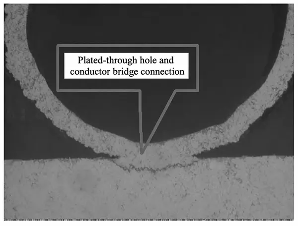
These methods identified the short-circuit point between a plated-through hole in one network and a conductor in another network. The analysis confirmed the fault location.
A horizontal microscopic cross-section of the short-circuit point is shown in Figure 1.
The short-circuit failure mode of this PCBA was a bridge between the plated-through hole and an adjacent conductor, caused by drilling misalignment; this defect is classified as a PCB manufacturing defect.
Generally, 100% continuity/non-continuity testing should be conducted before PCBs are shipped;
Defects of this type should not appear in shipped products.
The cause of the aforementioned issue is likely that quality management did not require 100% continuity/non-continuity testing, or that the testing failed to detect the defect; this constitutes a quality management issue rather than a technical issue.
Open Circuit Case Study
After the assembly of a certain PCB, it was discovered during debugging that the interconnect network between the mounting hole of one component and the pad of another component was open.
The investigation examined the PCB’s computer-aided manufacturing (CAM) data, performed segmented resistance measurements on the affected network, and conducted X-ray scanning.
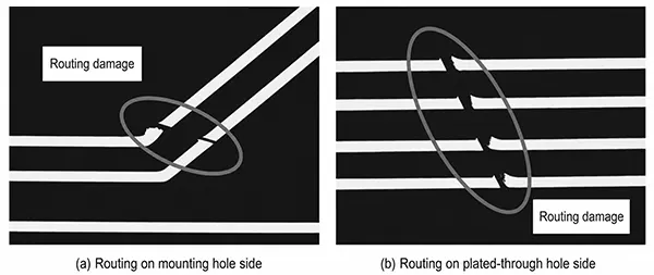
These analyses identified the open circuit in an inner-layer trace between the component mounting hole and a plated-through hole. The results confirmed the exact fault location.
A horizontal microscopic cross-section of the open trace is shown in Figure 2.
The open-circuit failure mode of this PCB was a break in the inner-layer conductor.
Observation of the cross-section revealed two breaks in the interconnect network trace, and similar breaks were also found in other adjacent network traces.
Analysis of the fracture morphology indicated that the breaks were caused by external scratches.
This defect is entirely human-induced. If it had originated during the manufacturing of the inner-layer conductors, it should have been rejected during subsequent automated optical inspection (AOI);
If it occurred during the lamination process, it should also have been rejected during the product’s continuity/non-continuity testing, thereby preventing the product from entering the shipped batch.
Therefore, this is a quality management issue rather than a technical issue.
CAF Case Study
A product failed after many years of use, manifesting as a low-resistance condition between a signal network and the ground network, suggesting a micro-short-circuit failure.
The investigation measured the resistance between the surface pads and plated-through holes in the failed signal network and the ground network.
It also performed short-circuit tracing and time-domain reflectometer (TDR) impedance analysis. These methods identified the micro-short circuit between the inner-layer conductors. The results confirmed the exact fault location.
The scanning electron microscope (SEM) image of a horizontal microtome section of the substrate at the micro-short-circuit region’s crack is shown in Figure 3;
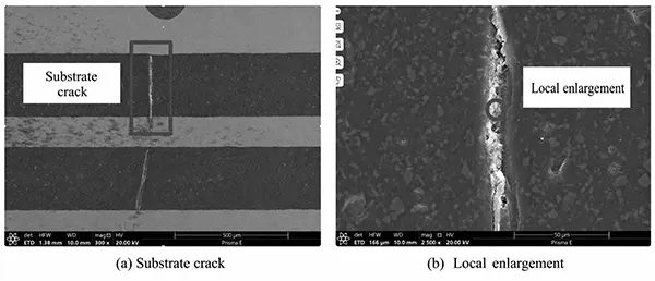
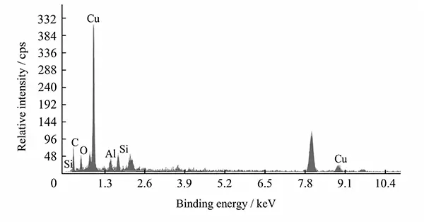
Figure 4 shows the energy-dispersive X-ray spectroscopy (EDS) image of the crack. Table 1 presents the results of the intelligent quantitative analysis.
This PCB micro-short-circuit failure mode is a typical case of CAF occurring between an inner-layer signal conductor and an adjacent ground network.
The investigation examined the morphology of the conductors in the CAF path and the substrate cracks.
The analysis identified scratches on the surface of the inner-layer conductors during PCB manufacturing as the root cause of the CAF.
Quality inspectors could have detected and eliminated this defect during the inspection of the inner-layer conductors.
Manufacturers could also have strengthened operating standards to prevent this defect. Either measure would have prevented the defect from creating a hidden risk to product reliability.
Therefore, this failure stems from inadequate manufacturing quality control rather than technical limitations.
| Element | Mass Fraction (%) |
|---|---|
| C | 29.08 |
| O | 7.48 |
| Cu | 54.25 |
| Al | 4.70 |
| Si | 4.48 |
Table 1. Quantitative Analysis Results of Energy Spectrum Analysis
PCB Quality Assurance Recommendations
The analysis examined the major failure modes, failure causes, and preventable factors described above.
The findings showed that stronger quality control throughout the entire PCB manufacturing process can effectively reduce the PCB failure rate.
Effective quality control should cover PCB design, process control, manufacturing, and inspection.
Considering the characteristics of PCB manufacturing and its product quality control requirements, the following recommendations support effective PCB quality assurance.
Collaborative Design
Design is the foundation of PCB quality and reliability.
For PCB products, the selection of upstream materials, intermediate component processing, electronic assembly of subassemblies, and the downstream system application environment all affect their performance and quality.
Therefore, PCB design should encompass material selection, structural design, manufacturing process design, electronic assembly processes, board-level subassembly, and quality inspection.
PCB designers must select appropriate materials and design structures based on the end product’s functional performance, application environment, and the manufacturer’s technical capabilities;
Establish reasonable inspection procedures and requirements in accordance with product quality needs;
And collaborate on the design with end-product designers, application stakeholders, PCB manufacturers, and electronic assembly manufacturers.
This ensures that the product not only meets functional performance requirements but also fulfills the criteria for manufacturability and cost-effectiveness.
Technical Status Control
The primary cause of PCB failure is defects in the manufacturing process; strengthening manufacturing quality control is the most effective measure to reduce manufacturing defects and improve product quality.
Manufacturers should manage PCB products as critical components and control them according to technical status items.
Manufacturers should conduct a first-article (or first-batch) qualification before pilot production or mass production.
They should also perform this qualification whenever key raw materials, production processes, or manufacturing parameters change.
The qualification process includes:
① Conducting comprehensive qualification inspections of the manufacturing process in accordance with relevant standards and design requirements;
② Assembling and debugging components to comprehensively verify the functionality of the printed circuit board assembly;
③ Confirming baseline elements such as manufacturing process documentation, process flows, key raw materials, quality inspection requirements, and inspection methods;
Finalizing the versions of process and technical documentation, and ensuring their accuracy, completeness, and validity.
Strict Control of the Manufacturing Process
As the integration density of electronic circuits continues to increase, PCB manufacturing processes and techniques are becoming increasingly complex.
All elements of the manufacturing process—people, machinery, materials, methods, environment, and testing—have a significant impact on product quality.
Effective product quality depends on a robust manufacturing quality management system.
Manufacturers should establish and continuously improve this system throughout the production process.
They should strictly follow standardized operating procedures and effectively manage every aspect of manufacturing, including material quality, personnel competence, process documentation, equipment condition, environmental conditions, and inspection standards.
Manufacturers should also strengthen personnel training and skills assessment.
They should improve communication and implementation of process requirements, maintain process and quality documentation, monitor production processes and environmental conditions, maintain equipment properly, and perform root-cause analysis of quality issues.
These measures help control the manufacturing process effectively and ensure consistent product quality.
Strengthening Quality Inspection
Effective and thorough quality inspection is a key guarantee for controlling quality during the manufacturing process and reducing product failure rates.
Given that the PCB production process is lengthy, the manufacturing techniques are complex, and there are numerous factors affecting quality, conducting quality inspections properly is all the more important.
First, manufacturers must strictly enforce quality inspections throughout the manufacturing process.
They should perform process inspections and finished product inspections in accordance with applicable standards, process documents, and customer technical requirements.
These inspections prevent defective products from leaving the factory because of inadequate quality control. They also reduce hidden risks that could affect product reliability.
Second, end-users should conduct thorough incoming material inspections and review the shipping inspection reports;
They should also perform necessary sampling and retesting of finished PCBs and associated test boards to verify the completeness, accuracy, and validity of the inspections.
Third, production personnel should conduct batch-based quality supervision and inspection.
Manufacturers should conduct periodic or quality consistency inspections for multiple batches or large production runs. These inspections monitor the stability of the manufacturing process and ensure consistent product quality.
Conclusion
As the core component of electronic devices, the quality of PCBs directly determines the performance and reliability of electronic products and complete systems.
An integrated quality assurance system that covers design, process, manufacturing, and inspection, together with full-process quality control, effectively reduces the failure rate of PCB products.
Effective quality control has consistently demonstrated its value, particularly in industries with high reliability requirements, such as medical, aerospace, automotive, and defense.
This article focuses on the major failure modes of PCBs and several typical failure cases, and proposes measures to strengthen PCB quality assurance.
The objective is to increase awareness of quality control among PCB designers, manufacturers, and users.
Greater attention to quality control helps reduce the failure rate of PCB products.
It also improves PCB product quality and enhances the overall quality and market competitiveness of electronic products.

