
Surface Mount Technology (SMT) is a core process in modern electronics manufacturing.
Thanks to its advantages of high density, high efficiency, and low cost, it has become the mainstream technology in the field of printed circuit board (PCB) assembly.
As electronic products evolve toward miniaturization and higher performance, component sizes are shrinking.
Meanwhile, solder joint pitch is continuously decreasing.
These trends place higher demands on the precision and reliability of the SMT process.
However, during SMT production, component detachment from the PCB surface occurs frequently.
Failures resulting from such detachment—such as cold solder joints and poor connections—have become one of the key challenges limiting product quality and yield.
Component detachment typically occurs during the reflow soldering stage or under subsequent mechanical stress (such as during testing or transportation).
In mild cases, it leads to functional failure; in severe cases, it can trigger systemic equipment failures.
Particularly in high-reliability fields such as automotive electronics and aerospace, such issues can have serious consequences.
Research indicates that component detachment is related to various factors.
These factors include soldering processes, solder joint corrosion, and mismatches in reflow soldering temperature profiles.
They also cover interfacial stresses induced by differences in the coefficient of thermal expansion (CTE) of materials, as well as external mechanical impacts.
Although existing research has explored the phenomenon of component detachment from multiple perspectives, most of these studies focus on detachment induced by solder‑joint defects.
By contrast, there is relatively little analysis addressing detachment caused by PCB board defects.
Therefore, this paper analyzes the causes of component detachment resulting from PCB board defects, clarifies the failure mechanisms through experiments, and proposes corresponding improvement measures.
Test Methods and Analysis of Results
This paper analyzes the causes of component detachment in batches of failed PCBs during SMT production at a certain factory.
After undergoing two reflow cycles in the SMT process (with a maximum temperature of 265°C), the component detachment rate for these failed PCBs was approximately 1.5%.
This study adopted multiple testing and analysis methods to explore the causes of pad detachment on failed PCBs.
The applied techniques include metallographic section observation, scanning electron microscopy (SEM), and energy-dispersive spectroscopy (EDS).
Water absorption testing, thermal stress testing, thermomechanical analysis (TMA), as well as differential scanning calorimetry (DSC) were also utilized for the analysis.
Visual Inspection
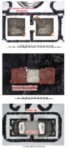
A stereo microscope (model SQ900) was used to examine the locations where components had come loose on the failed PCB;
The results are shown in Figure 1.
Some components on the failed PCB had come loose, with the separation interface located within the substrate beneath the PCB pads;
In addition, solder balls encased in flux were widely visible on the board surface in the SMT area.
Cross-Section Analysis
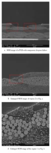
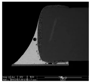
Cross-sections were prepared from the detached components and pads, as well as from the failed PCB at the component detachment site, and examined using an SEM (model InspectF50).
The results are shown in Figure 2. The interface where the components detached is located within the resin beneath the PCB pads or between the resin and the glass fiber bundles;
In some areas, cracks extend from the glass fiber bundles into the substrate.
The cross-sectional morphology of the detached components and pads is shown in Figure 3, revealing a significant number of voids within some solder joints.
Analysis of the Detachment Interface
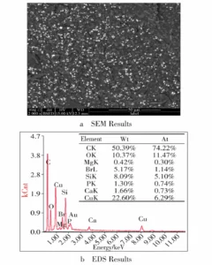
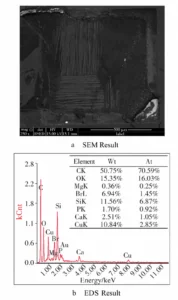
To further analyze the adhesion at the component detachment interface, an SEM (model InspectF50) and EDS (model Apolloxp) were used to directly observe and analyze the interface where the component pad had detached.
The morphology is shown in Figure 4. Resin residue was present on the bottom of all detached pads, and copper protrusions were visible in some areas.
This phenomenon may result from inadequate lamination between the copper foil and the resin.
However, the copper protrusions are distributed only in peripheral regions and cover a small area.
This observation suggests that inadequate lamination between the copper foil and the resin is not the primary cause of component detachment for this case.
The PCB side corresponding to the detachment interface at the bottom of the component pad is shown in Figure 5.
Glass fibers are exposed on the PCB surface, and no significant resin adhesion is observed on the glass fibers.
Combined with the results of the cross-section analysis, it can be concluded that the delamination interface of the failed PCB component pad is primarily located between the glass fiber and the resin.
Furthermore, the wetting of the glass fiber by the resin is relatively insufficient, resulting in a relatively weak bond between the substrate and the resin.
When the thermal stress during the SMT process exceeds the internal bonding strength of the board, delamination and cracking are likely to occur in the soldered areas of the PCB.
Water Absorption Rate
Water absorption rate testing was performed on failed bare PCBs in accordance with the method specified in IPC-TM-6502.6.2.1A:1998:
First, the bare PCB was baked at 105°C for 1 hour and then weighed to obtain m1;
Then they were immersed in deionized water for 24 hours; after wiping the surface moisture from the bare PCBs, they were weighed again to obtain m2.
As required, three samples were tested in parallel.
Water Absorption Rate = (m2 – m1) / m1 × 100%
The water absorption test results are shown in Table 1.
These results indicate that the PCB’s water absorption rate meets the technical requirement of ≤0.35% specified in IPC-4101C for copper-clad epoxy-glass laminates and their bonding sheets.
| Sample | m₁ / g | m₂ / g | Water Absorption | Technical Requirement | Conclusion |
|---|---|---|---|---|---|
| 1 | 13.1520 | 13.1768 | 0.19% | ≤ 0.35% | Pass |
| 2 | 13.2678 | 13.2989 | 0.23% | ≤ 0.35% | Pass |
| 3 | 13.5213 | 13.5625 | 0.30% | ≤ 0.35% | Pass |
Table 1: Water absorption test results
Thermal Stress Analysis
Following the method specified in IPC-TM-6502.6.8E:2004, thermal stress testing was conducted on failed bare PCBs under the following conditions:
SAC305 solder was used, and soldering was performed at 288°C for 10 seconds.
Two bare PCBs that failed after water absorption testing and two bare PCBs that failed after being baked at 125°C for 6 hours were selected for testing.
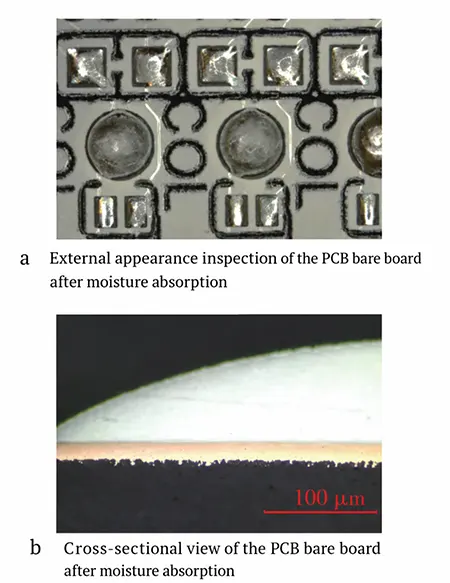
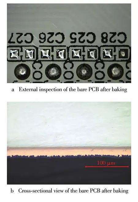
After the test, the bare PCBs underwent visual inspection and cross-sectional analysis; the results are shown in Figures 6–7.
No obvious delamination or blistering was observed on either the moisture-absorbed or oven-dried bare PCBs.
This indicates that even with a certain degree of moisture absorption, the bare PCBs can still withstand the soldering heat specified in the IPC-4101C standard.
TMA Testing
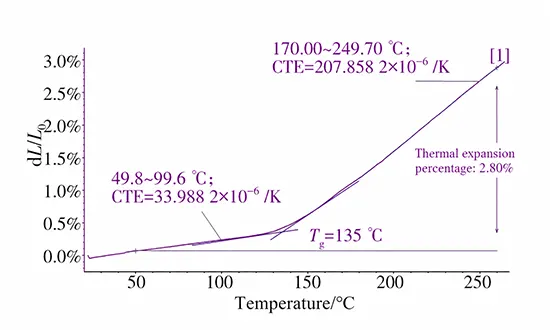
To further analyze the stress sources causing component and pad detachment on the failed PCB during the SMT process, this paper conducted simulated testing on the failed PCB using a TMA (model TMA402F3).
Prior to testing, the sample was baked at 105°C for 2 hours; after cooling to room temperature, it was heated at a rate of 10°C/min to 265°C to complete the scanning test. The test results are shown in Figure 8.
The glass transition temperature (Tg) of this failed PCB is approximately 135°C.
The coefficient of thermal expansion (CTE) below Tg is 33.99 × 10⁻⁶/K, while the CTE above Tg is 207.86 × 10⁻⁶/K—the latter being approximately six times that of the former.
The peak temperature of the SMT process is approximately 260°C, which is significantly higher than the Tg of this PCB.
It can therefore be concluded that the resin matrix of the failed PCB expanded and deformed due to heat during the SMT heating process, thereby generating internal stress.
Analysis of Resin Curing Degree
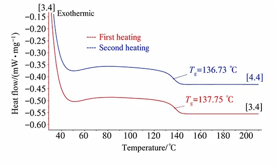
To further analyze the degree of resin curing in the failed PCB, and in accordance with the ISO 11357-5:2025 standard, DSC testing was performed on the resin.
The temperature range was set to 35–210°C, with a heating rate of 10°C/min.
The results are shown in Figure 9. Compared to the second heating curve, no distinct exothermic peak was observed in the resin of the failed PCB during the first heating process.
This indicates that the resin in the failed PCB had already fully cured.
Failure Cause Analysis
Macroscopic Failure Phenomenon and Preliminary Cause Exclusion
The pads on the failed PCB components have come loose, and resin residue is present on the underside of all the detached pads; exposed copper teeth are visible in some areas.
This may be caused by poor bonding between the copper foil and the resin (during the lamination process);
However, since the copper teeth are distributed only in the peripheral areas and cover a small area, it indicates that poor bonding between the copper foil and the resin is not the primary cause of component detachment in this case.
Curing degree tests indicate that the resin in the failed PCB has fully cured;
Therefore, resin abnormalities are also not the cause of component detachment.
Core Failure Mechanism of PCB Component Detachment
1. Thermal Stress Induced Delamination and Failure Mechanism of PCB Substrate
The detachment of component pads on the failed PCB mainly occurs at the interface between glass fiber and resin.
The wetting performance between glass fiber and resin is relatively poor. This condition leads to low bonding strength of the PCB substrate.
During the SMT heating process, the resin expands and deforms due to heat; during the subsequent cooling phase, the board should have reverted to its original shape.
Two-terminal components such as resistors and capacitors are mounted on the PCB surface.
Their solder joints gradually solidify during the cooling stage.
This process forms a rigid connection between the components and the PCB substrate.
Component solder joints impose structural constraints on the PCB. Therefore, the resin on the component-mounted side fails to deform normally.
In contrast, the resin on the non-component side can deform and recover its original shape.
This discrepancy generates axial stress along the thickness direction of the PCB.
When this stress exceeds the internal bonding strength of the board, delamination and cracking occur in the soldered areas of the PCB, ultimately leading to failure.
2. Interface Characteristics of Component Detachment and Substrate Bonding Defects
A comprehensive analysis of the interface characteristics at the point of component detachment reveals that:
Portions of the detachment interface are located between the glass fiber bundles and the resin;
The resin surface exhibits smooth indentations from the glass fibers; and no significant resin adhesion is observed on the surface of the glass fiber bundles.
This indicates insufficient wetting of the glass fibers by the resin and weak bonding strength between the substrate and the resin.
When the axial stress in the thickness direction of the PCB is high, delamination between the resin and the glass fiber bundles is more likely to occur and spread to other areas, ultimately causing component detachment.
3. Adverse Effect of Moisture Absorption on PCB Failure
Furthermore, although the PCB’s water absorption rate meets the requirements of the technical specifications, the adverse effects of moisture absorption cannot be ruled out.
The widespread presence of solder balls on the failed PCB surface and a high number of voids in the solder joints suggest that the PCB may have been exposed to moisture to some extent.
Once a PCB absorbs moisture, the “popcorn” phenomenon is likely to occur during the SMT process.
Improvement Measures and Verification Results
At this point, the axial stress in the thickness direction of the PCB increases, leading to cracking.
It is recommended to apply a coating to the glass fiber surface (such as an aminosilane coupling agent) to improve wettability between the glass fiber and the resin and enhance bond strength.
Additionally, PCB panels should be baked as much as possible before use to minimize the impact of moisture on stress.
Subsequently, the customer used glass fiber coated with an amino-silane coupling agent during PCB fabrication and baked the panels before use;
As a result, component detachment issues did not recur during the SMT process.
Conclusion
In summary, insufficient wetting between the glass fiber strands and the resin in the PCB is the primary cause of component detachment from the PCB surface.
Additionally, the PCB may have absorbed a certain amount of moisture, which increases stress during the soldering process and ultimately leads to the detachment of the PCB pads.

