
Printed circuit boards (PCBs) serve as carriers for electronic components, and their flatness directly affects the quality of surface mount technology (SMT) and solder joint reliability.
PCB warpage after SMT not only causes component misalignment and cold solder joints but can even lead to solder shorts or open circuits, severely affecting product performance and lifespan.
In actual production, the causes of PCB warpage are highly complex, involving multiple factors such as material properties, laminate structure, copper residue distribution, and process flows.
Particularly against the backdrop of the widespread adoption of lead-free soldering processes, the increase in soldering temperatures places even higher demands on PCB heat resistance and dimensional stability.
Therefore, effectively controlling PCB warpage after SMT has become an urgent issue for PCB manufacturing and electronic assembly companies.
Based on actual post-SMT PCB warpage issues encountered in a company’s production process, this paper designs multiple sets of comparative experiments and systematically evaluates the impact of factors such as materials, baking processes, and structural design on board warpage, with the aim of providing optimization recommendations for engineering practice.
Description of the Issue
A PCB product for a new project exhibited significant warpage after SMT.
Automated optical inspection (AOI) revealed that the defect rate for component flatness exceeded 80%.
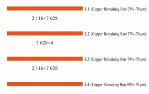
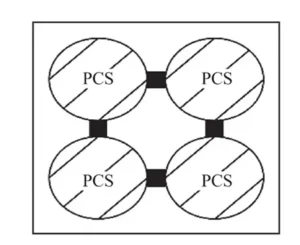
The product incorporates the following design features: the use of relatively high-cost Material A (Tg ≥ 170 °C, Td = 351 °C), a four-layer board with a 70 μm (2 oz) copper base layer, and a stack-up and panelization design, as shown in Figures 1 and 2.
Cause Analysis and Troubleshooting
Based on existing PCB product designs, and in accordance with manufacturing processes and design specifications, this study analyzes and investigates the causes of PCB warpage occurring after SMT.
The investigation results indicate that material selection, post-molding process steps, and the design of open areas between PCBs are the primary factors influencing PCB warpage after SMT. See Table 1 for a detailed analysis.
| No. | Possible Cause | Investigation / Findings | Determination |
|---|---|---|---|
| 1 | Asymmetric Stackup | The product is a 4-layer PCB, with a copper thickness of 70 μm on each layer. The interlayer PP is 7628 + 2116, forming a symmetrical structure. | Not the Root Cause |
| 2 | Large Difference in Copper Remaining Rate Between Layers | The copper remaining rates of L1, L2, L3, and L4 are between 79% and 68%, with a maximum difference of 11%. This is well below the 45% maximum allowable difference specified by the design requirements and therefore meets the design specification. | Not the Root Cause |
| 3 | Improper Material Selection | The selected material, Type A, has a Tg ≥ 170°C. A higher-performance material may be required to meet the board warpage resistance requirements. | Possible Root Cause |
| 4 | Excessive Open Area Between PCS Regions | There are large areas without copper between the PCS regions. These areas lack process-side support, which may cause stress concentration in the intermediate areas and lead to PCB warpage. | Possible Root Cause |
| 5 | Abnormal Incoming Material Tg Value | A finished PCB sample was sent to the laboratory for Tg testing. The actual test results were Tg = 176.05°C and 175.22°C, with ΔTg = 0.83°C, indicating no abnormality. | Not the Root Cause |
| 6 | Unbaked Panels After Material Cutting | According to the production work instructions and actual production records, this PCB had an additional baking process after panel cutting. No abnormality was found. | Not the Root Cause |
| 7 | Abnormal Lamination Program | Production records show that the core materials and PP used for PCB lamination comply with the process specifications. No abnormality was found. | Not the Root Cause |
| 8 | Mismatch in Post-Forming Process Steps | The post-forming process is: Forming → Final Cleaning → Final Quality Control (FQC) → Surface Treatment → Final Quality Assurance (FQA) → Packaging → Shipment. The baking process is missing. Without baking, PCB stress cannot be properly released, and heating during SMT production may cause the PCB to warp. | Possible Root Cause |
| 9 | No Warpage Inspection Before Shipment | According to shipment records, the PCB undergoes a 100% warpage inspection before shipment and meets customer requirements. No abnormality was found. | Not the Root Cause |
Table 1. Analysis of possible causes of board warping problem
Possible Causes Based on Experimental Validation
Based on the findings of the above investigation, and to systematically analyze the factors affecting board warpage, this paper designed three sets of comparative experiments to examine the effects of material selection, the design of open areas between PCSs, and post-molding process steps, respectively.
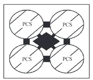
The experimental designs are shown in Table 2. In Design 2, additional connection points were added between the PCSs of Material A, as shown in Figure 3.
| Option | Condition 1 | Condition 2 | Condition 3 |
|---|---|---|---|
| Option 1 | Material A | No connections between PCS regions | Add post-forming bakingb |
| Option 2 | Material A | Add connections between PCS regions | No post-forming baking |
| Option 3 | Material Ba | No connections between PCS regions | No post-forming baking |
Note: “a” indicates that Material B is a higher-performance material grade with Tg ≥ 180 °C and a Td base of 355 °C;
b indicates that an additional baking process is added after molding, resulting in the following sequence: molding → cleaning of finished products → baking (170 °C, 2 h) → FQC testing → surface treatment → …
The Impact of the Post-Forming Baking Process
For PCBs that were not baked before SMT, the warpage defect rate detected by AOI after SMT exceeded 80%.
For PCBs baked according to Solution 1, the warpage defect rate detected by AOI after SMT was 0%.
This demonstrates that, under conditions where the material and structure remain unchanged, adding a post-molding baking process can successfully resolve the issue of board warpage.
Post-molding baking helps release residual stress within the PCB, particularly mechanical stress accumulated during processes such as lamination, drilling, and molding.
Through the baking process, the internal structure of the material stabilizes, making it less prone to deformation during the high-temperature SMT process.
This process is simple, easy to implement, and low-cost, making it suitable for widespread adoption in mass production.
The Effect of Inter-PCS Connection Methods
For PCBs that originally lacked reinforced inter-board connections, the warpage defect rate in AOI inspection after SMT exceeded 80%.
After implementing Solution 2 to add inter-board connections, the warpage defect rate in AOI inspection after SMT was 0%.
This demonstrates that, without changing the materials or the curing process, adding inter-PCS connections can effectively suppress board warpage.
The connection points between PCSs act as reinforcing ribs, improving the overall rigidity of the panels and reducing the risk of deformation during forming, handling, and SMT processes.
Particularly in multi-panel designs, properly configuring these connection points not only improves flatness but also enhances production efficiency and reduces damage during the handling of individual panels.
Impact of Material Selection
In Scenario 3, under identical process conditions (no connection points, no baking), replacing Material A with Material B reduced the defect rate for board warpage detected by AOI after SMT from over 80% to 0%, eliminating the warpage issue.
This indicates that a material’s thermal stability is one of the key factors affecting board warpage.
Material B has higher Tg (≥180 °C) and Td (355 °C) values, exhibiting better resistance to thermal deformation during the high-temperature SMT soldering process.
Materials with high Tg values can maintain a higher modulus, reducing the release of interlaminar stress caused by mismatched coefficients of thermal expansion, thereby effectively suppressing board warpage.
Discussion
Comprehensive Analysis and Mechanism Exploration
The experimental results indicate that PCB warpage following SMT is the result of the combined effects of multiple factors.
There is a coupled relationship among the thermal properties of the materials, structural design, and process control.
(1) Material-dominated: During the high-temperature soldering process, the material’s thermal expansion characteristics and Tg value determine its ability to resist thermal stress.
(2) Process-Assisted Type: The baking process can effectively release residual stress and improve the dimensional stability of the material.
(3) Structural Reinforcement Type: The placement of connection points can increase the overall rigidity of the board, thereby reducing the risk of deformation.
In actual production, if material selection is limited, this can be compensated for by optimizing the process or structural design;
If process conditions are limited, priority should be given to selecting high-performance substrates or enhancing the structural design.
Engineering Recommendations
Based on the results of this experiment, the following engineering recommendations are proposed.
(1) Add a post-molding baking process: Incorporate this into the standard production process, particularly for panels with complex structures and greater thickness;
(2) Optimize the design of PCS connection points: Appropriately increase the number of connection points to enhance structural rigidity without compromising panel separation efficiency;
(3) Prioritize the use of high-performance materials: Especially for multilayer boards, thick copper boards, or high-temperature soldering processes, materials with a Tg ≥ 180 °C and a Td value of approximately 355 °C are recommended.
Conclusions
Through systematic testing and research on PCB warpage issues following SMT, this paper draws the following conclusions:
(1) A post-molding baking process can effectively relieve residual stress and is a simple and effective method for reducing board warpage;
(2) Increasing the number of connection points between PCBs can enhance structural rigidity and reduce the risk of deformation;
(3) The thermal properties of the material are a key factor influencing board warpage; high-performance materials (Tg ≥ 180 °C; Td = 355 °C) exhibit better resistance to deformation during high-temperature soldering;
(4) These three factors can work synergistically; in actual production, they should be flexibly combined and applied based on product structure and process conditions.
Although the issue of board warpage is complex, it can be effectively controlled through scientific experimental design and process optimization.
The results of this study provide an experimental basis for improving board warpage issues after SMT and hold significant engineering application value.

