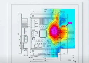
Heat dissipation is a key aspect of PCB thermal design. The goal of heat dissipation is to implement appropriate measures when component temperatures exceed the reliability-guaranteed temperature, thereby lowering the temperature back within the reliability operating range.
PCB heat dissipation primarily relies on three mechanisms: thermal conduction, convection, and radiation.
Material Selection
The substrate used in PCB manufacturing is the medium that comes into direct contact with components, and its heat dissipation capability directly affects the overall thermal performance of the system.
The best way to address heat dissipation is to enhance the PCB’s own heat dissipation capability—specifically, its ability to conduct or radiate heat away from heat-generating components—which makes the selection of the substrate particularly important.
First, when selecting PCB materials, we must differentiate based on the product’s intended use and operating environment to determine the appropriate board type.
A board’s heat dissipation capability is closely linked to two parameters: thermal conductivity and heat resistance.
There are five major types of PCB materials available on the market: paper-based substrates, composite substrates, epoxy-glass fiber cloth substrates, resin-coated copper foil (RCC) used in HDI, and specialty substrates.
Paper-Based Substrates
Paper-based substrates (FR-1, FR-2, FR-3), formally known as phenolic resin-impregnated paper substrates, are the least expensive.
However, they have strict soldering temperature requirements, are prone to moisture absorption and bubbling, and tend to yellow when exposed to temperatures exceeding 260 °C, indicating poor heat resistance.
Their thermal conductivity is well below 1.0 W/m·K.
Composite Substrates
Composite substrates (CEM-1, CEM-3) are so named because they consist of two materials: a glass fiber cloth base combined with a wood pulp paper base.
They represent an upgrade over paper-based substrates, offering improved performance and strong mechanical processability, while costing less than glass fiber cloth substrates.
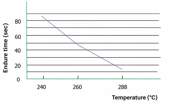
However, as shown in the thermal shock curve, they can only withstand 260 °C for 50 seconds.
In terms of heat resistance alone, there is no significant improvement compared to paper-based substrates, and their thermal conductivity is also less than 1.0 W/m·K.
Epoxy Glass Fiber Cloth Substrate
Epoxy glass fiber cloth substrates, commonly referred to as FR-4, feature high mechanical and dielectric properties, good heat and moisture resistance, and excellent machinability.
Its heat resistance is particularly outstanding; at 288 °C, it can maintain its integrity for 150 seconds without delamination or bubbling.
In thermal stress testing, its peel strength is also high, reaching 1.5 N/mm. Its thermal conductivity is approximately 1.0 W/m·K.
Among these, FR-4 with a high glass transition temperature (TG) exhibits even greater resistance to high temperatures.
FR-4 is more expensive than the two materials mentioned earlier.
HDI
In most cases, HDI is designed using RCC (resin-coated copper) material, i.e., resin-coated copper foil.
It features high toughness and is easy to handle; Its smooth surface is suitable for fine circuits; and it has extremely high peel strength.
However, because the surface copper layer is thin and the dielectric consists solely of resin without glass fiber, it is significantly less rigid than other board types and also has considerably lower thermal conductivity.
Special Substrates
Among special substrates, two types are widely used: ceramic substrates and aluminum substrates.
Ceramic substrates, as the name implies, are special copper-clad laminates formed by embedding copper foil within a ceramic dielectric.
This material offers excellent electrical insulation, high thermal conductivity, superior soft solderability, and high adhesion strength.
It is generally used in military and aerospace applications and is relatively expensive.
Aluminum substrates are metal-based copper-clad laminates with good heat dissipation capabilities.
They are generally designed as single-sided boards and are primarily used in LED light boards and low-end power supply boards; for high-end applications, they are also designed as double-sided boards, though very few are used as multilayer boards.
Aluminum substrates minimize thermal resistance, providing excellent thermal conductivity, electrical insulation, and machinability.
They can withstand voltages up to 4,500 V and have a thermal conductivity of 3.0 W/m·K or higher.
Considering the various substrate materials mentioned above, it is clear that paper-based and composite substrates no longer meet the requirements of current heat treatment applications, even though they offer the advantage of low cost;
HDI RCC substrates have limitations in practical use, and their heat dissipation capabilities are also quite poor;
Ceramic and aluminum substrates are certainly the most recommended among these materials, as they offer absolute advantages in both heat dissipation and heat resistance.
However, these two materials are expensive, so their use must be carefully considered based on the specific product requirements;
Epoxy-glass-fiber-reinforced substrates cannot dissipate heat as effectively as ceramic or aluminum substrates. However, they cost significantly less than both alternatives. Their moderate heat dissipation performance meets the needs of general circuit designs.
They are also the most widely used and in-demand PCB substrate materials on the market today.
Component Layout
Staggered and dispersed arrangement. When laying out components during PCB design, heat-generating components should be separated from general-purpose components and temperature-sensitive components.
Sufficient airflow channels for heat dissipation should be left around heat-generating components, and these components should be arranged in a staggered and dispersed manner.
When components with different thermal characteristics are mounted together, it is best to place components that generate more heat downwind and those that generate less heat upwind.
When components with similar heat resistance levels are arranged together, the general rule is to place components with high power consumption and poor heat dissipation on the upwind side.
The thermal capacity of the PCB surface should be distributed evenly; avoid concentrating high-power-consumption components in one area.
If this cannot be avoided, place shorter components upstream of the airflow and ensure sufficient cooling airflow passes through the area with concentrated heat dissipation;
Keep heat transfer paths as short as possible and maximize the heat transfer cross-sectional area.
Do not place components with high heat generation or high current in the corners or along the edges of the PCB.
Install heat sinks whenever possible, and position them away from other components to ensure unobstructed heat dissipation pathways.
Component layout should account for the impact of thermal radiation on surrounding parts.
Heat-sensitive components (including semiconductor devices) should be kept away from heat sources or isolated from them.
Optimal Trace Layout Design
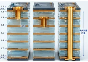
Since the resin in the substrate has poor thermal conductivity, while copper foil traces and vias are good thermal conductors, improving the copper foil yield and increasing the number of thermal vias are the primary methods for heat dissipation.
To determine a PCB’s heat dissipation capacity, it is necessary to calculate the equivalent thermal conductivity of the PCB’s insulating substrate, which consists of materials with varying thermal conductivities.
The thicker the copper foil, the higher the copper foil retention rate; the more layers there are, the greater the equivalent thermal conductivity, and the better the PCB’s heat dissipation performance.
Under the heat sinks of high-heat components, place as many vias as possible in a uniform distribution to conduct as much heat as possible through the vias to the inner layers and the copper plane on the back side;
On the component side, expand the GND or other copper areas connected to the heat sink pads to utilize the top-layer copper for heat dissipation;
Ensure that vias are connected to the copper foil on the plane layers as much as possible; if the area is not GND, a small patch of copper foil can be added separately, as appropriate, to enhance heat dissipation;
If necessary, on the back side, directly beneath high-heat components, further utilize the bottom surface for heat dissipation by removing solder mask and stencil patterns from the copper layer;
When routing PCB traces to improve heat dissipation, adopt design solutions that include wide traces, thick copper foil, thin boards, multiple layers, large areas of copper plating, and the addition of via holes.
Selecting Components Wisely
Even before PCB design begins, the selection of components can have a certain impact on a product’s heat dissipation performance.
Thermal Characteristics and Application Limitations of THD Components
THD-packaged components are through-hole components.
These components have fewer pins, and after soldering, the component body does not lie flush against the PCB; therefore, their thermal coupling with the board is minimal.
The heat generated by these components dissipates through their surfaces, so using them in environments with high airflow provides better thermal performance.
However, since these packages are discrete components, using them in large quantities occupies significant PCB space and prevents the design from being made smaller, resulting in certain limitations in their application.
Classification and Thermal Features of SMD Packages
SMD (Surface Mount Device) packages generate significant heat and are a key focus in thermal design.
These devices typically have a large number of pins and high pin density.
After soldering, the device body lies flush against the PCB, making it closely tied to the board’s overall heat dissipation.
There are many types of SMD packages; from a thermal perspective, they are classified into two categories: leaded packages and ball grid array (BGA) packages.
BGA (Ball Grid Array) devices belong to the ball-type category; heat dissipation from the board itself can generally be ignored, as heat is primarily dissipated through the package surface.
Devices that generate significant heat typically require the addition of a heat sink or heat spreader.
SOP (Small Outline Package) devices belong to the lead-type category and have very poor heat dissipation performance;
The main factor affecting their heat dissipation is the high heat generated by the device itself, which is difficult to dissipate.
Since current component packages are relatively small, heat dissipation through the component surface alone is largely ineffective.
Recommended Component Selection Strategies for Thermal Optimization
If SMD components are selected, it is advisable to choose packages with a heat sink pad in the center of the component.
This allows heat to be transferred to the PCB via the heat sink pad and then dissipated through the large copper foil area on the PCB.
Additionally, selecting component types that allow for the installation of heat sinks facilitates heat dissipation in later stages.
Ensure Unobstructed Heat Dissipation Pathways
Make full use of component layout, copper planes, cutouts, and heat dissipation holes to establish rational and effective low-thermal-resistance pathways, ensuring that heat is efficiently dissipated from the PCB.
Designing heat dissipation through-holes and blind holes can effectively increase the heat dissipation area, reduce thermal resistance, and improve the power density of the circuit board.
To reduce thermal resistance during heat transfer, apply thermal interface material to the contact surfaces between high-power components and the substrate to improve heat transfer efficiency.
Areas with components mounted on both sides of the board are prone to localized overheating.
To improve heat dissipation, a small amount of fine copper particles can be mixed into the solder paste;
After reflow soldering, this creates a slight elevation at the solder joints beneath the components.
This increases the gap between the components and the PCB, enhancing convective heat dissipation.
Other Measures for PCB Thermal Design
Use multilayer boards in PCB design to increase the number of power and GND planes.
Heat can be dissipated through large areas of copper foil, preventing it from concentrating in a specific area and damaging components in that region.
During the design process, vias are used to establish electrical interconnections between different layers.
Connecting multiple GND planes together expands the heat dissipation area, which can significantly improve the PCB’s heat dissipation capability.
When connecting high-heat-dissipation components to the substrate, thermal resistance between them should be minimized as much as possible.
To better meet thermal performance requirements, thermal conductive materials (such as a layer of thermal silicone grease) can be applied to the bottom surface of the chip, and a sufficient contact area should be maintained to facilitate heat dissipation from the component.
When connecting components to the substrate, keep the lead lengths as short as possible;
When selecting high-power components, consider the thermal conductivity of the lead material and choose leads with the largest possible cross-sectional area; opt for components with a higher number of pins.
If necessary, add heat sinks and fans to the components.