In addition to component selection and circuit design, good PCB design is also a very important factor in electromagnetic compatibility.
The key to PCB EMC design is to minimize the return path area as much as possible and ensure that the return current flows in the intended direction.
The most common return current issues stem from gaps in the reference plane, changes in the reference plane layer, and signals flowing through connectors.
Bypass capacitors or decoupling capacitors may resolve some of these issues, but the total impedance of the capacitors, vias, pads, and traces must be taken into account.
The following section introduces EMC PCB design techniques from three perspectives: PCB layering strategies, layout techniques, and routing rules.
PCB Layering Strategies
In PCB design, thickness, via processes, and the number of layers are not the key to solving problems.
A well-designed layer stackup is crucial for ensuring bypassing and decoupling of power buses, minimizing transient voltages on power or ground planes, and shielding signal and power electromagnetic fields.
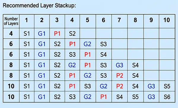
From the perspective of signal routing, a good layering strategy involves placing all signal traces on one or several layers that are immediately adjacent to the power or ground planes.
For power distribution, a good layering strategy requires the power plane to be adjacent to the ground plane, with the distance between them kept as small as possible—this is what we refer to as the “layering” strategy.
1. The projection plane of the routing layer should fall within the area of its return plane layer.
If the routing layer is not within the projection area of its return plane layer, signal traces may extend beyond the projection area during routing, leading to “edge radiation” issues.
This also increases the signal loop area, resulting in increased common-mode radiation.
2. Avoid placing routing layers adjacent to one another whenever possible.
Parallel signal traces on adjacent routing layers can cause signal crosstalk;
If adjacent routing layers are unavoidable, we should appropriately increase the interlayer spacing between these two routing layers and decrease the spacing between the routing layer and its signal return loop.
3. Avoid overlapping the projected planes of adjacent plane layers.
When the projected planes overlap, the coupling capacitance between layers can cause noise to couple between them.
Multilayer Board Design
When the clock frequency exceeds 5 MHz or the signal rise time is less than 5 ns, a multilayer board design is generally required to effectively control the signal loop area.
We should follow the principles below when designing multilayer printed circuit boards:
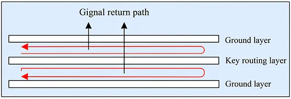
1. Critical routing layers (layers containing clock lines, buses, interface signal lines, RF lines, reset signal lines, chip select signal lines, and various control signal lines) should be adjacent to a continuous ground plane, preferably positioned between two ground planes, as shown in Figure 1.
Critical signal lines are generally either highly radiative or extremely sensitive;
Routing them close to a ground plane reduces the area of their signal loops, thereby decreasing their radiation intensity or improving their immunity to interference.
2. Designers shall recess the power plane relative to its adjacent ground plane, with a recommended recess range of 5H to 20H.
Recessing the power plane relative to its return ground plane can effectively suppress the “edge radiation” problem, as shown in Figure 2.
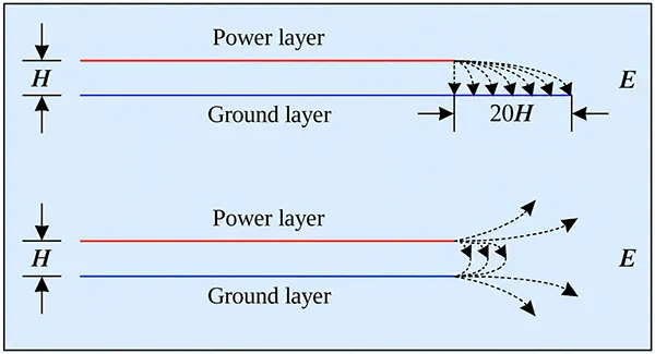
In addition, the main power supply plane on a single-board circuit (the most commonly used power supply plane) should be adjacent to its ground plane to effectively reduce the loop area of the power supply current, as shown in Figure 3.
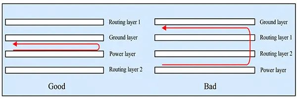
3. Are there any signal lines operating at ≥50 MHz on the TOP and BOTTOM layers of the PCB?
If so, it is best to route the high-frequency signals between the two plane layers to suppress their radiation into the surrounding space.
Single-Layer and Double-Layer Board Design
When designing single-layer and double-layer boards, the primary focus should be on the design of critical signal lines and power lines.
Ground traces must run adjacent to and parallel with power traces to minimize the area of the power current loop.
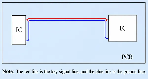
For single-layer boards, route “Guide Ground Lines” on both sides of critical signal traces (Figure 4).
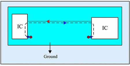
For double-layer boards, lay a solid ground plane beneath critical signal traces.
Alternatively, implement “Guide Ground Lines” as used in single-layer designs (Figure 5).
The “protective ground lines” on both sides of critical signal lines not only reduce the signal loop area but also prevent crosstalk between signal lines.
PCB Layout Techniques
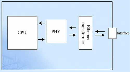
When designing a PCB layout, you should strictly adhere to the design principle of placing components in a straight line along the signal path and avoid back-and-forth routing as much as possible, as shown in Figure 6.
This helps prevent direct signal coupling, which can degrade signal quality.
Basic Layout Principle for Signal Path Routing
Additionally, to prevent mutual interference and coupling between circuits and electronic components, the placement of circuits and the layout of components should follow the following guidelines:
1. When designing a “clean ground” interface on a PCB, place filtering and isolation components within the isolation region between the clean ground and working ground.
This prevents filtering or isolation components from coupling with each other through the plane layers, which would weaken their effectiveness.
Furthermore, designers shall not place any components other than filtering and protection devices on the “clean ground.”
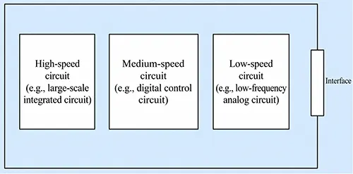
2. When multiple circuit modules are placed on the same PCB, digital and analog circuits, as well as high-speed and low-speed circuits, should be laid out separately to prevent mutual interference between them.
In addition, when high-, medium-, and low-speed circuits are integrated on one PCB, designers should adopt the layout rules illustrated in Figure 7 to avoid outward radiation of high-frequency noise via interfaces.
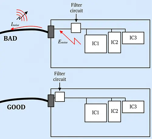
3. Designers should place the power-input filter circuit of the PCB near the connector to avoid recoupling of the filtered signal.
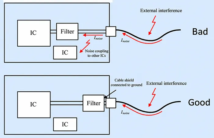
4. Placing filter, protection, and isolation components close to the interface, as shown in Figure 9, can effectively achieve protection, filtering, and isolation.
When both filter and protection circuits exist at an interface, follow the rule of “protection first, then filtering”.
Protection circuits suppress external overvoltage and overcurrent. If placed behind the filter circuit, overvoltage and overcurrent may damage the filter circuit.
Circuit input and output traces may produce mutual coupling effects. Such coupling will weaken the performance of circuit filtering, isolation and protection.
Therefore, reasonable layout design is essential for electronic circuits. The input and output traces of filtering, isolation and protection circuits should avoid mutual coupling.
Layout Requirements for Sensitive Circuits and High-Current Loops
5. Keep sensitive circuits or components (such as reset circuits) at least 1000 mils away from the edges of the board, especially the edges on the side with connectors.
6. Place energy-storage and high-frequency filtering capacitors near circuit units or components subject to significant current fluctuations (such as the input and output terminals of power supply modules, fans, and relays) to reduce the loop area of high-current paths.
7. Designers shall place filter components adjacent to one another to avoid secondary interference to the filtered circuit.
Placement Rules for High-Radiation Components
8. Designers shall place high-radiation components including crystals, oscillators, relays and switching power supplies at least 1000 mils away from the PCB interface connectors.
This allows interference to radiate directly outward or to couple as current onto external cables for outward radiation.
PCB Routing Rules
Component selection and circuit design are essential for electromagnetic compatibility.
Proper PCB routing also serves as a critical influencing factor for EMC performance.
The PCB constitutes an indispensable part of the entire electronic system. Optimizing EMC via reasonable PCB routing brings no extra costs to finished products.
It is important to remember that poor PCB routing can cause more EMC problems rather than eliminate them; in many cases, even the addition of filters and components cannot resolve these issues.
Ultimately, the entire board may have to be rerouted.
Therefore, developing good PCB routing habits from the start is the most cost-effective approach.
The following section introduces some general rules for PCB routing and design strategies for power, ground, and signal lines.
Finally, based on these rules, improvement measures are proposed for a typical air conditioner printed circuit board (PCB) circuit.
Routing Separation
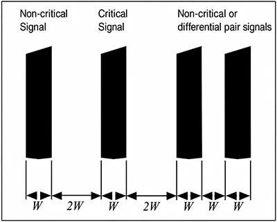
The purpose of routing separation is to minimize crosstalk and noise coupling between adjacent traces on the same layer of a PCB.
The 3W specification stipulates that all signals (clock, video, audio, reset, etc.) must be isolated from one another—line-to-line and edge-to-edge—as shown in Figure 10.
To further reduce magnetic coupling, the reference ground should be routed near critical signals to isolate coupling noise generated on other signal lines.
Shielding and Shunt Lines
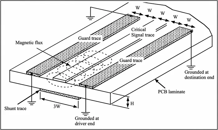
The use of shunt and shielding lines is a highly effective method for isolating and protecting critical signals, such as system clock signals in a noisy environment.
In Figure 21, parallel or shielding lines within the PCB are routed alongside the critical signal lines.
Shielding lines not only isolate the signal from coupled magnetic flux generated by other signal lines but also prevent the critical signal from coupling with other signal lines.
Shunt lines differ from shield lines: shunt lines require no ground termination, while shield lines must be grounded at both ends.
For multilayer PCBs, designers may ground shield lines periodically to further reduce crosstalk coupling.
Power Trace Design
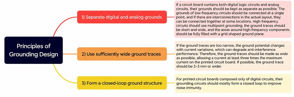
Based on the current level of the printed circuit board, increase the width of the power traces as much as possible to reduce loop resistance.
At the same time, align the routing of the power and ground traces with the direction of data transmission; this helps enhance noise immunity.
For single-sided or double-sided PCBs with lengthy power traces, designers shall add decoupling capacitors to ground every 3000 mils using a combination of 10 μF and 1000 pF capacitors.
Ground Trace Design
Signal Line Design
For critical signals, if the PCB contains inner signal layers, designers should route critical signals such as clock signals on inner layers and select the most suitable routing layer preferentially.
Additionally, critical signal lines must not cross partition boundaries—including gaps in the reference plane caused by vias or pads—as this would increase the signal loop area.
In addition, designers shall route critical traces at least 3H away from the reference plane edge (H denotes the trace height above the reference plane) to mitigate edge radiation.
High-radiation traces including clock lines, buses and RF lines, as well as sensitive traces such as reset, chip select and system control signals, should be separated from interface output traces.
This prevents interference from strongly radiating signal lines from coupling into the output signal lines and radiating outward;
It also prevents external interference introduced by the interface output signal lines from coupling into the sensitive signal lines, which could cause system malfunctions.
Designers shall route differential signal traces on the same layer with equal lengths and parallel alignment to preserve consistent impedance, and no other traces can be placed between the differential pair.
This is because ensuring that the common-mode impedance of the differential pair is equal improves its immunity to interference.
Using the above routing guidelines, we optimized the layout of a typical air-conditioner PCB, as illustrated in Figure 12.
Overall, PCB design can improve EMC performance as follows:
Designers shall finish rational return path planning before PCB routing.
This design strategy greatly facilitates the reduction of EMI radiation. Layout adjustments such as routing layer optimization incur no additional cost in the pre-routing stage.
It serves as the most cost-effective method to improve system EMC performance.
Conclusion
Effective PCB EMC design requires coordinated control of the layer stackup, component layout, return paths, and routing.
The primary goal is to minimize signal and power loop areas while maintaining short, continuous, and predictable return paths.
Proper placement of ground and power planes, separation of sensitive and high-radiation circuits, appropriate filtering and shielding, and controlled routing of critical signals can significantly reduce electromagnetic interference and crosstalk.
A rational PCB design should also consider connector interfaces, reference-plane continuity, differential-pair routing, power and ground trace design, and the physical placement of filtering and protection components.
These measures help prevent unwanted coupling and reduce both conducted and radiated interference.
Most importantly, EMC optimization should begin during the PCB design and pre-routing stages rather than after EMC problems appear.
Careful return-path planning, suitable layer-stackup design, disciplined component placement, and proper routing rules can improve EMC performance without significantly increasing manufacturing costs.
A systematic EMC design approach therefore provides an effective and economical way to improve the reliability and electromagnetic compatibility of the entire electronic system.