
Electronic information technology has advanced rapidly since the 21st century. Various fields, including consumer electronics, communication equipment, automotive electronics, and industrial control, continuously demand high-performance and highly integrated electronic products.
As the core component of electronic equipment, printed circuit boards (PCBs) undertake basic electrical interconnection functions.
They have gradually become critical components that determine system thermal management, mechanical stability and signal integrity.
Traditional substrates represented by FR-4 exhibit low thermal conductivity. Their thermal conductivity is only 0.2–0.3 W/(m·K).
Such performance fails to satisfy the heat dissipation demands of high-power chips.
Typical devices include central processing units (CPUs), graphics processing units (GPUs) and power amplifiers.
Heat accumulation can lead to component performance degradation, reduced lifespan, and even functional failure, becoming a bottleneck that limits technological progress in electronic devices.
At the same time, the trend toward thinner, lighter, and higher-density electronic products places greater demands on the mechanical stability and local current-carrying capacity of PCBs.
Modern electronic systems, including servers, base stations, and new energy vehicle electronic control units, widely adopt PCBs.
These rigorous application scenarios require PCBs to withstand high current loads and high-frequency vibrations.
They also need to endure severe thermal cycling environments. Traditional PCB structures are no longer capable of adapting to such harsh operating conditions.
To address these challenges, the industry continues to explore new materials and processes.
Embedded copper block technology stands out as an efficient thermal solution.
It possesses outstanding comprehensive performance. Pure copper delivers a high thermal conductivity of approximately 398 W/(m·K).
It also features excellent electrical conductivity and superior mechanical strength.
For these advantages, this technology has attracted extensive research and industrial attention.
In this study, based on the method by which copper blocks are incorporated into PCBs, the embedded copper block technology is classified into two categories: inlaid copper blocks and embedded copper blocks.
The former involves mechanically embedding copper blocks into pre-milled grooves in the PCB, while the latter involves embedding copper blocks into the core board during the lamination process to form an integrated structure.
This study systematically summarizes the technical details of embedded copper block processes.
It clarifies the complete process flows and manufacturing capabilities of the technology.
It also defines its applicable engineering scenarios. This work provides both theoretical support and practical guidance.
It benefits the design and mass production of high-reliability PCBs.
Introduction to Copper-Insert PCBs
The copper-insert PCB process is a technique that uses mechanical force to embed prefabricated copper inserts into straight grooves pre-milled on the surface of a PCB.
The core of this process lies in the “insertion” action, which relies on an interference fit between the copper insert and the groove walls, as well as the protruding teeth structure on the side walls of the insert, to achieve mechanical interlocking.
This process is typically performed during the back-end of PCB manufacturing (such as after molding) and is suitable for applications with high thermal dissipation requirements but strict cost constraints, as shown in Figures 1 and 2.
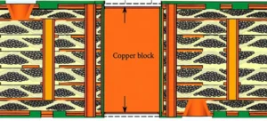
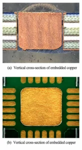
Copper inserts dissipate heat directly through their exposed surfaces, effectively reducing the thermal resistance between the heat source and the heat sink.
The embedded copper block process features simple operational procedures.
This effect barely influences upstream manufacturing processes. The industry widely adopts copper inserts to enhance local heat dissipation performance.
They are applicable to both double-sided and multilayer PCBs. This technology delivers outstanding application flexibility.
It is especially suitable for high-variety and small-batch production modes.
Process Flow and Methods for Embedding Copper Blocks
Prefabrication
Technicians precisely machine penetrating rectangular through-slots via CNC milling at PCB heat-dissipation-enhancing positions, typically underneath chips.
Meanwhile, engineers prefabricate solid copper blocks with slightly larger dimensions than the target slots and design unique serrated or knurled structures on their side walls.
Press-Fit Assembly
Using specialized press equipment, a prefabricated copper block is forcefully pressed vertically into a PCB slot.
The key to this process is the “interference fit” (where the copper block is slightly larger than the slot), and the copper block is forced into the slot under high pressure.
Forming an Interlocking Connection
The protruding teeth on the side walls of the copper block “bite” tightly into the resin-glass fiber of the substrate;
This interference fit creates an extremely robust mechanical interlocking structure between the copper block and the substrate.
This connection does not rely on adhesives or soldering; its stability is ensured purely by the physical structure.
Manufacturing Details
(1) Copper Block Requirements:
① The finished dimensions of the PCB milled groove should be 0.1 mm smaller overall than the copper block dimensions to ensure a tight fit;
② The R-corner of the protruding teeth on the copper teeth is 0.5 mm, and the R-corner of the recessed teeth is 1.5 mm; the height tolerance of the copper teeth is ±0.05 mm;
③ The length and width tolerances for the copper teeth are ±0.05 mm, and the thickness tolerance is ±0.03 mm;
④ The copper block has a fillet radius of 0.5 mm and a chamfer angle of 60°.
(2) Milling Copper Grooves:
① Use a “rough milling + finish milling” process to machine the slots for the copper inserts;
The rough milling cutter is ϕ1.6 mm, the finish milling cutter is ϕ1.0 mm, and the feed rate for finish milling is 0.6 m/min;
② Use a milling machine with a precision of ±0.075 mm for production; the laminate stack height must be ≤3.0 mm, and a cover plate must be applied;
③ For the first board, control the slot dimensions within ±3 mil (1 mil =0.025 4 mm); in-process quality control (IPQC) must monitor slot dimensions within ±3 mil.
(3) Copper Block Insertion:
① Clean the press head before each insertion to prevent indentations on the copper block surface, and use a press to insert the copper block into the PCB slots;
② Inspect the flatness of the copper block on the first board, controlling it to ±0.075 mm on the insertion surface and ±0.10 mm on the protruding surface (for multilayer boards, +0.10 to −0.15 mm);
③ IPQC shall conduct random inspections of the copper block flatness at a rate of 1 board per 15 boards;
The number of surface indentations must be ≤3, and the copper block surface must be free of ink and other foreign matter residues;
④ Wear gloves when handling boards and avoid touching the copper block area; do not allow boards to collide or be stacked during transportation.
Manufacturing Process for Copper-Inlaid Circuit Boards
Manufacturing Process
1. Double-Sided Boards—Non-Electrolytic Copper Groove Copper Inlay
Main Process: Cutting, Drilling, Hole Metallization and Plating, Circuit Pattern Formation, Solder Mask Application, Surface Treatment → Milling Grooves, Forming, Electrical Testing → Copper Inlay → Pickling, Final Inspection, Packaging.
This process mills grooves after completing PCB surface treatment, retains unplated inner groove walls, and fixes copper blocks entirely through mechanical compression.
2. Double-Sided Boards—Copper Blocks Embedded in Milled Grooves
Main Process: Cutting, drilling → Milling grooves → Hole metallization and electroplating, circuit patterning, solder mask application, surface treatment, forming → Embedding copper blocks → Pickling, electrical testing, final inspection, packaging.
Features: The grooves are milled before electroplating; the copper coating on the inner walls enhances electrical connectivity and bonding strength.
3. Multi-layer PCBs with Embedded Copper Blocks
Main Process: Material cutting → Inner layer patterning, lamination → Drilling → Milling slots → Via metallization and electroplating → Embedding copper blocks → Outer layer patterning, solder mask application, surface treatment, forming, electrical testing, acid washing, final inspection, and packaging.
Process characteristics: Operators embed copper blocks after finishing lamination, drilling, and electroplating procedures, and then transfer outer layer patterns sequentially.
Therefore, the copper blocks must be able to withstand subsequent wet processes.
Manufacturing Capabilities (Subject to Adjustment Based on Factory Equipment Capabilities)
(1) Copper Inlay for Double-Sided Boards: Copper block dimensions—short side ≥ 5 mm, long side ≤ 7 mm, thickness 0.90–1.2 mm;
Copper block flatness: ±0.075 mm on the embedded surface and ±0.10 mm on the protruding surface.
(2) Copper-embedded multilayer boards: Copper block dimensions—short side ≥ 5 mm, long side ≤ 40 mm, thickness ≥ 1.2 mm;
Copper block flatness—±0.075 mm on the embedded surface and +0.10/−0.15 mm on the protruding surface.
Technical Specifications
This study defines the finished product performance requirements according to the IPC-6012 Class 2 standard and lists key selected specifications in Table 1.
| No. | Test Item | Test Conditions | Acceptance Criteria |
|---|---|---|---|
| 1 | Thermal Stress | 288°C, 10 s, 3 cycles | No delamination between the copper block and PCB |
| 2 | Lead-Free Reflow Soldering | 3 cycles | No delamination between the copper block and PCB |
| 3 | Warpage | Finished Product Test | ≤ 0.75% |
| 4 | Hole Wall Copper Thickness | Cross-Section Analysis | Customer Requirements |
| 5 | Height Difference Between Copper Surface and Board Surface | Cross-Section Analysis | ≤ ±0.05 mm |
| 6 | RF Circuit Accuracy | Line Width Tester | ≤ ±25 μm |
Table 1 Selected performance requirements for PCBs with embedded copper blocks
Applications of Copper-Embedded PCBs
This process achieves a chemical-mechanical bond between the copper block and the PCB substrate, offering higher reliability, superior flatness, and greater design integration.
This technology is highly applicable to heat-sensitive and space-limited scenarios.
These scenarios require efficient heat dissipation with strict space and cost constraints.
Typical application fields cover multiple high-power electronic devices.
They include high-power light-emitting diodes (LEDs) and automotive electronic control units (ECUs).
Power supply modules and industrial control systems also adopt this technology.
It applies to power amplifiers and RF modules in communication equipment.
Furthermore, it suits high-performance routers and adapters in consumer electronics.
Introduction to Buried Copper Block Circuit Boards
The buried copper block process adopts prefabricated solid copper blocks as embedded components and permanently encapsulates them inside substrates during PCB lamination.
To implement this fabrication route, technicians first mill grooves on core boards at designated embedding positions and perform window cutting on corresponding prepreg (PP) materials for pretreatment.
The fabrication proceeds with a high-temperature and high-pressure lamination process.
Liquid resin flows out from the prepreg during this stage. The flowing resin fully fills the gaps between copper blocks and slot walls.
This process forms robust bonding between copper blocks and dielectric layers, building a highly reliable integrated board structure.
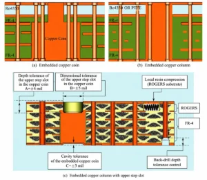
Engineers classify embedded copper blocks into two primary design categories.
The first type is the standard rectangular straight copper block, also known as the copper column.
The second type is the variable-thickness stepped copper block, namely the copper pedestal.
These two structures are illustrated in Figure 3. They are designed to satisfy diverse thermal management and structural requirements.
The embedding method also offers flexibility: through-embedding allows the copper block to pass through the board layers and protrude on both sides for heat dissipation on both sides;
Blind embedding, on the other hand, exposes the copper block on only one side to preserve space for high-density routing on the surface layer.
This process significantly enhances the heat dissipation capacity of high-power chips and optimizes internal grounding and power distribution, thereby improving the PCB’s mechanical stability and electrical performance.
Process Flow and Methods for Embedded Copper Blocks
Process Flow for Manufacturing Printed Circuit Boards with Embedded Copper Blocks
Core Process: Material Cutting → Inner Layer Tracing → Inner Layer Punching → Milling Grooves in the Core Board → Milling PP Windows → Automated Optical Inspection (AOI) of Inner Layers → Laminating (Embedded Copper Blocks) → Ceramic Board Grinding → Laser Ablation → Sandblasting → Drilling → Post-Processing.
Method for Manufacturing Circuit Boards with Embedded Copper Blocks
1. Copper Blocks
(1) Adjust the thickness of the copper blocks through trial runs to ensure the height difference between the copper blocks and the PCB meets customer requirements.
(2) Incoming Inspection: The side walls of the copper blocks (purple copper or red copper) must be perpendicular to the surface, without chamfers;
They must be smooth and free of damage marks; and the edges must be free of defects such as notches, bumps, or dents.
Operators must individually package each copper block and store it with foam separators.
Dimensions and thickness must comply with drawing requirements, with length and width tolerances of ≤±0.05 mm (to avoid affecting the potting width) and thickness tolerances of ≤±0.03 mm.
(3) Browning: Use specialized fixtures to brown the copper blocks; bake at 105 °C for 1 hour; handle with care while wearing sulfur-free gloves;
Technicians must avoid stacking to prevent surface scratches and impact damage.
They inspect the browning quality of copper block surfaces and sidewalls;
Browning treatment applies only to one single side and all sidewalls, while the opposite side requires no treatment. The process allows only one round of rework.
2. Milling PP Sheets
(1) PP Milling Strip Design: For blind buried pads (exposed on one side), do not mill grooves in the PP where it contacts the bottom of the copper block;
For buried copper pads, mill grooves in the PP where it contacts the stepped surface of the copper block according to the dimensions of the smaller copper pad;
Technicians compensate the groove dimensions for prepreg (PP) regions corresponding to copper block embedding areas by adding 0.215 mm to the single-side dimension specified in the original drawings.
(2) Design a 5-hole positioning system; clamp the PP between two smooth plates (each stack secured with crimp tape before transport) with a thickness of 0.5 mm or greater.
Use a rough milling + finish milling process, with a feed rate set to 0.3 m/min and 15 sheets per stack; replace the cover plate and milling cutter after each pass, and ensure the slot dimensions in the core board are ≤±0.10 mm.
(3) There must be no residual adhesive in the slots; copper blocks must fit properly to ensure correct dimensions.
3. Milling the Core Board
(1) Core board milling design: Technicians adjust the milling dimensions of core board slots according to surface treatment conditions.
For unplated slot walls that contact copper blocks, they expand each side of the milled slot by 0.112 mm relative to the copper block dimensions specified in the original drawings.
For copper-plated slot walls, they increase the dimension of each milled slot side by 0.112 mm plus the copper plating thickness, based on the original copper block design dimensions.
(2) Project and punch 5 rivet holes for positioning. For laminated board thicknesses ≤3.0 mm, use a blank plate the same size as the core board as the cover plate.
Employ a rough milling followed by finish milling process, ensuring the core board slot dimensions are within ±0.075 mm.
(3) Technicians ensure slot edges remain free of burrs to facilitate normal copper block insertion and maintain dimensional accuracy.
4. Laminating
(1) Laminating stack: Base plate / Kraft paper / Steel plate / Cushion pad / Aluminum sheet / Release film / PCB (copper side facing up) / Release film / Aluminum sheet / Cushion pad / Steel plate / Kraft paper / Cover plate.
(2) After the copper block is placed in the slot, ensure its surface is level with the PCB and flat, with no skewing or warping.
Use the pressing procedure corresponding to PP.
(3) Technicians may use new aluminum sheets only once. They thoroughly clean these sheets with a waxed cloth and reject any sheets with dents, creases, or other defects.
(4) Technicians conduct visual inspection of resin flow uniformity after lamination and carry out cross-section analysis.
They verify that resin fully fills the periphery of the copper block without gaps or pinholes, and confirm proper alignment of both the copper block and sub-board.
When milling the board edges, remove the rivet holes to prevent the ceramic brush from being damaged during board grinding.
5. Laser Ablation
(1) Using the original copper block’s slot dimensions—with a 0.20 mm inward offset on each side—as the baseline, create a laser-drilled strip extending 5 mm into the interior of the copper block, ensuring that the laser does not burn the edges of the copper block.
(2) After sanding the board, use laser drilling to ablate and remove residual adhesive from the surface of the copper block.
If any adhesive remains, sand it down with 600-grit or finer sandpaper; the width of residual adhesive at the edges of the copper block must be ≤0.25 mm or as specified by the customer.
(3) After ablation, visually inspect for any ablation misalignment and check the gap at the junction between the copper block and the PCB;
Test the depth of the difference between the copper block and the board surface to ensure it is ≤±0.075 mm.
6. Ceramic Grinding Plates
When grinding the plates, position them with the slots facing down to prevent insufficient drying.
After grinding, conduct a 100% inspection of the copper blocks to check for residual adhesive on their surfaces; IPQC will randomly inspect 8 out of every 30 plates.
7. Drilling Holes in the Copper Block
(1) Use X-ray to mark 5 reference holes for positioning.
Technicians select individual holes on copper blocks and drill them with dedicated cutting tools.
They drill one panel (PNL) per stack and adopt specialized drilling parameters optimized for copper substrates.
(2) After drilling, inspect the hole edges to ensure they are burr-free, with a burr height ≤0.05 mm (no thread snagging when a cotton glove is slid over the edge), and no residual copper wires inside the holes.
Use a rack to bake the board (glass transition temperature: Tg+10 °C, 2 hours).
Process Capabilities for Embedded Copper Blocks
(1) Embedding Methods: Through-hole (exposed on both sides), blind (exposed on one side).
(2) Shape and Dimensions of Embedded Copper Blocks: Straight copper blocks (copper pillars), stepped copper blocks (copper platforms); minimum dimensions: 3 mm × 3 mm; maximum dimensions: 30 mm × 40 mm.
(3) Height difference between copper blocks and board surface: ±0.05 mm.
(4) Drilling holes in copper blocks: Thickness 1.0 mm, drill diameter 0.5 mm; thickness 1.5 mm, drill diameter 0.8 mm;
Thickness 2.0 mm, drill diameter 1.0 mm; thickness 2.5 mm, drill diameter 1.5 mm.
(5) Spacing: ≥9 mm between adjacent copper blocks; ≥0.5 mm between holes and the edge of the copper block; ≥0.4 mm between holes on the same copper block.
Comparison of Embedded Copper Blocks and Buried Copper Blocks
See Table 2 for a comparison of circuit boards with embedded copper blocks and those with buried copper blocks.
| Comparison | Embedded Copper Block PCB | Buried Copper Block PCB |
|---|---|---|
| Advantages | ① High thermal conductivity and heat dissipation, while saving board space. ② Simple manufacturing process, high efficiency, and low cost. | ① High thermal conductivity and heat dissipation, while saving board space. ② More complex manufacturing process and higher cost, but high reliability. |
| Disadvantages | ① Copper block geometry affects the embedding result and may damage the copper block or groove walls, resulting in a high scrap rate. ② Dimensional deviations between the milled groove and copper block can prevent close contact, causing severe copper block wear and shortening product life. ③ The copper block relies on mechanical force for embedding. Flatness may not meet conventional component-side and solder-side requirements. Excessive height differences can reduce heat dissipation. | ① An excessively loose or tight fit between the copper block and milled groove affects lamination resin filling and bonding strength. ② During lamination, controlling copper block and FR-4 core flatness within ±0.025 mm is difficult, but ±0.05 mm is achievable. ③ Residual resin on the copper block requires removal, increasing cost and risk. ④ Height differences between the copper block and FR-4 core during lamination may cause insufficient resin fi |
Table 2. Comparison of Advantages and Disadvantages Between Embedded Copper Block PCBs and Buried Copper Block PCBs
Conclusion
Based on PCB manufacturing practices, this paper systematically analyzes the underlying mechanisms and process windows of the embedded copper block process and identifies the following quantifiable technical points.
Point 1
Precise control of the “interference fit + interlocking protrusions” in the embedded copper block process:
Specify that the copper block dimensions should have a negative compensation of 0.10 mm on each side relative to the milled groove;
The protruding tooth R-angle should be 0.5 mm and the recessed R-angle 1.5 mm; and the combination of rough and finish milling (ϕ1.6 mm + ϕ1.0 mm) and a fine milling feed rate of 0.6 m/min.
This method effectively improves the flatness of mechanically embedded copper blocks.
The flatness tolerance is controlled within ±0.075 mm on the embedded surface.
The protruding surface achieves a flatness tolerance of ±0.10 mm. For multilayer boards, the flatness range is from +0.10 mm to −0.15 mm.
Traditional copper embedding produces uneven gaps, which cause local warpage and high interfacial thermal resistance.
The proposed process successfully eliminates these inherent defects.
Second Point
This study develops an integrated manufacturing process for embedded copper blocks.
The process combines stepped copper platform, laser ablation and ceramic grinding technologies.
Conventional embedded copper processes suffer from stubborn resin overflow and severe copper surface height deviations.
To solve these problems, this study establishes a complete closed-loop process chain.
The procedure includes core board and PP window milling with a single-sided compensation of 0.112–0.212 mm.
It is followed by lamination treatment, ceramic grinding and laser ablation.
This study defines strict dimensional tolerances for copper blocks. The length and width tolerance of the copper block is ≤±0.05 mm.
Its thickness tolerance is ≤±0.03 mm. Laser ablation extends 5 mm into the copper block with a baseline retraction of 0.20 mm.
With these settings, the height difference between the copper block and board surface is controlled within ±0.05 mm.
The residual adhesive width at the edges is kept ≤0.25 mm.
These improvements greatly enhance the machinability and long-term reliability of embedded copper boards in subsequent manufacturing processes.
Third Point
This study focuses on parameter optimization for secondary drilling on copper blocks.
Drilling on copper blocks frequently causes typical defects, including burrs, hole misalignment and rough hole walls.
Targeted drill bit parameters and lamination schemes are proposed based on copper block thickness classification.
The schemes cover two installation states: copper-block-down placement and bare board coverage.
Corresponding design rules are established. The minimum hole diameter is set to 0.5 mm, and the hole-to-hole spacing is 0.4 mm.
The distance from the hole edge to the copper block edge is specified to be no less than 0.5 mm.
This research fills the technical specification gap for secondary precision machining in copper block regions.
This study is conducted based on practical production conditions. It proposes quantifiable and reproducible process parameters and control strategies for embedded copper block technology.
It provides a feasible technical solution. This solution supports high-efficiency heat dissipation and high-reliability PCB manufacturing.

