
Today, I’d like to share some information on PCB trace width, calculating PCB trace width, and the relationship between PCB trace width and current.
What is PCB Trace Width?
Trace width is one of the most critical factors in PCB design. Anyone who frequently designs circuits knows that trace width issues come up often.
Some designers who are just starting out and lack experience tend to use the default trace widths provided by PCB layout software.
For experienced designers, the default trace widths serve as a useful reference, but they may use their experience to determine that certain traces are too narrow—especially for power and ground connections.
What Are Traces?
PCB traces are fine conductive copper lines placed on a non-conductive or insulating substrate, used to transmit signals and power throughout the circuit.
Copper traces have a specific width, which we call the trace width, and a specific height or thickness.
Typically, the thickness of the copper layer on a PCB is fixed and determined by the specifications of the PCB manufacturer.
For a typical PCB, the most common copper thickness is 35 mil, which is equivalent to 1 oz/sq ft.
Therefore, in the design process, we can only control the trace width.
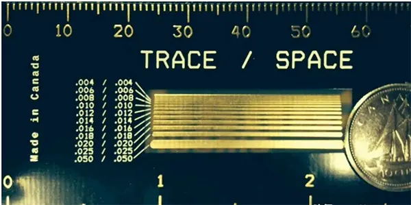
For most manufacturers, the minimum trace width is 6 mil or 0.152 mm, primarily due to limitations in the etching process and target yield;
However, to allow for some tolerance, trace widths of 0.254–0.3 mm are typically used.
What Factors Are Critical to Trace Width?
Signal Traces
Signal traces are the traces that carry data.
In digital or analog signals, varying trace widths typically do not have a significant impact on simple PCB designs, but they are critical in RF/analog and high-speed digital designs.
In such designs, trace impedance is an important consideration because trace width and impedance are inversely proportional.
Power Traces
On the other hand, power traces require more attention because they are responsible for supplying power to every component in the circuit.
There are two reasons for using different trace widths in PCB design.
1. Current Carrying Capacity
Current carrying capacity is the first and most obvious reason.
Why? The relationship between conductor width and current carrying capacity is straightforward.
The cross-sectional area of a trace and the allowable temperature rise determine how much current the trace can carry.
The cross-sectional area of a trace is also directly proportional to the copper thickness and trace width.
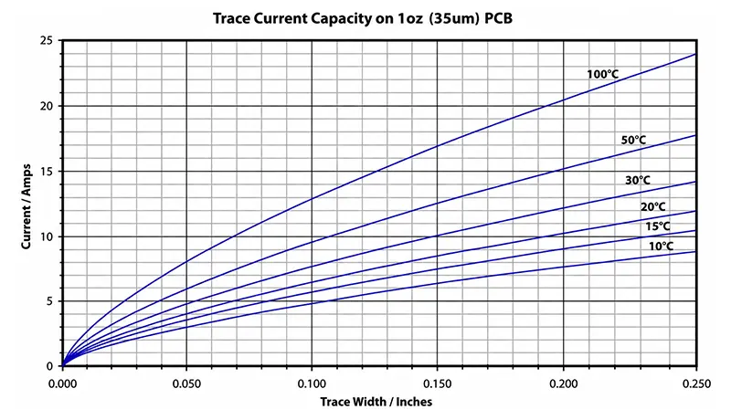
When we increase the current flowing through any given trace, the temperature also rises.
The trace must be able to handle this increase in temperature. One simple way to ensure this is to increase the width of the trace.
The IPC-2152 standard serves as the starting point for determining trace widths;
These standards use empirical data to generate tables for calculating current limits for a given temperature rise.
The PCB trace width tables are well-suited for evaluating PCB trace widths and cross-sectional areas.
The table below can be used to effectively determine the upper limit of the allowable current in a trace.
Given the infinite variables in a PCB stackup, you will need to use simulation to analyze the PCB in order to accurately measure current density and temperature rise.
However, for most typical circuit boards, the IPC tables are sufficient.
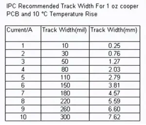
The figure below shows several trace widths and their corresponding current values, which will limit the temperature rise to 10°C with a copper weight of 1 ounce per square foot.
Some online tools can calculate the trace width required to carry a rated current while keeping the trace temperature below a specified limit.
Actual results may vary depending on the application and conditions.
2. Trace Impedance
High-speed circuits may require specific spacing and impedance to minimize crosstalk, coupling, and reflections.
Sensitive data lines, such as RF/analog traces and high-speed traces, must be calculated.
For high-frequency signals, such as those in the GHz band, PCB traces function as more than simple connections.

Every copper trace has a certain amount of series inductance and internal resistance, which can easily be overlooked in simple, low-speed designs.
However, in high-speed designs, trace inductance, copper surface roughness, and the skin effect increase, which may affect the performance of the circuit board.
In addition, each signal trace exhibits some capacitance between its return path and other nearby traces.
Trace Width and Signal Reflection
Signal reflection is a fundamental issue in high-performance electronic circuit design.
The phenomenon in which certain portions of a transmitted signal are reflected back toward the source is called signal reflection; signal reflection can lead to signal distortion and oscillations.
Signal reflection in a PCB depends largely on the shape and routing of the traces.
Whenever a trace changes direction, shape, or interfaces with a component, trace discontinuities come into play.
For example, when a trace bends at a 90° angle, the trace width changes significantly.
At the bend, the trace width is 1.414 times the actual trace width.
This variation in trace width causes a change in impedance, which in turn leads to signal reflection.
Professional PCB designers are aware of these issues and therefore avoid sharp bends and uneven trace widths.
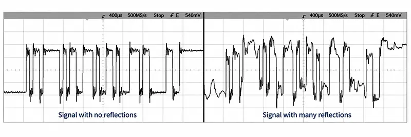
If left unaddressed, these factors can significantly reduce the system’s overall performance because impedance varies at different points along the signal path.
Trace coupling—especially when signals cross planes and gaps—can cause crosstalk.
A trace width calculator can help you determine how to derive the appropriate trace width. However, many factors must be considered, such as:
Trace current-carrying capacity.
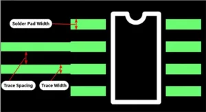
The spacing and dimensions of the component pads connected by the traces.
The spacing between traces.
In addition to trace width, the spacing between traces must also be considered to prevent short circuits and ensure maximum space between components for proper functionality.
PCBs are typically small due to production cost considerations.
However, if a board is too small, it may be difficult to route traces and maintain adequate spacing between them.
How to Calculate PCB Trace Width?
Use a PCB Trace Width Calculator
You can use a trace width calculator to determine the trace width based on current capacity.
However, you’ll need to provide design specifications to the calculator, including the maximum current flowing through the trace (in amperes), the total length of the path, and the temperature rise caused by trace resistance.
Once the specifications are provided, the calculator will automatically generate the calculated trace width, which is typically the minimum required width.
This allows current to flow safely without causing damage to the PCB.
You may notice that inner-layer trace widths are wider than those on the outer layers because they tend to generate more heat.
Due to convection, the outer layers do not accumulate as much heat.
For safety reasons, it is recommended to use the inner-layer trace width throughout the entire PCB.
Using the Equations
1. PCB Trace Width Table
The PCB trace width table can help you determine the trace width for your PCB and provides insight into the effects of current-carrying capacity and temperature rise.
Please refer to the table below.
The table below shows the maximum safe current capacity (A) for different PCB trace widths, copper thicknesses, and allowable temperature rises.
| Trace Width (inches) | 10°C / 0.5 oz | 10°C / 1 oz | 10°C / 2 oz | 20°C / 0.5 oz | 20°C / 1 oz | 20°C / 2 oz | 30°C / 0.5 oz | 30°C / 1 oz | 30°C / 2 oz |
|---|---|---|---|---|---|---|---|---|---|
| 0.01 | 0.5 | 1 | 1.4 | 0.6 | 1.2 | 1.6 | 0.7 | 1.5 | 2.2 |
| 0.015 | 0.7 | 1.2 | 1.6 | 0.8 | 1.3 | 2 | 1 | 1.6 | 3 |
| 0.02 | 0.7 | 1.3 | 2.1 | 1 | 1.7 | 3 | 1.2 | 2.4 | 3.6 |
| 0.025 | 0.9 | 1.7 | 2.5 | 1.2 | 2.2 | 3.3 | 1.5 | 2.8 | 4 |
| 0.03 | 1.1 | 1.9 | 3 | 1.4 | 2.5 | 4 | 1.7 | 3.2 | 5.5 |
| 0.05 | 1.5 | 2.6 | 4 | 2 | 3.6 | 6 | 2.6 | 4.4 | 7.3 |
| 0.075 | 2 | 3.5 | 5.7 | 2.8 | 4.5 | 7.8 | 3.5 | 6 | 10 |
| 0.1 | 2.6 | 4.2 | 6.9 | 3.5 | 6 | 9.9 | 4.3 | 7.5 | 12.5 |
| 0.2 | 4.2 | 7 | 11.5 | 6 | 10 | 11 | 7.5 | 13 | 20.5 |
| 0.25 | 5 | 8.3 | 12.3 | 7.2 | 12.3 | 20 | — | — | 24* |
2. Formula for PCB Trace Width
According to the definition in IPC-2221, you can determine the trace width of a PCB using the formula for calculating the allowable current through the trace. The process is as follows:
I = k * AT^0.44 * A^0.725
| represents current and is treated as a constant
AT refers to the temperature rise
A is the cross-sectional area of the trace.
Now, we can rearrange the formula to derive the trace width by determining the cross-sectional area required to safely carry the selected current.
Area [mils²] = (Current [amps] / (k * (Temperature Rise [°C])⁰.⁴⁴))^(¹/⁰.⁷²⁵)
k = 0.048
Next, consider the trace thickness to determine the required width.
Width [mils] = Area [mils²] / (Thickness [oz] * 1.378 [mils/oz])
This formula applies to currents ranging from 0 to 35 A, allowing for a temperature rise from 10°C to 100°C.
It accommodates trace widths up to 400 mils, and you can use copper thicknesses ranging from 0.5 to 3 ounces.
By substituting 2 A into the above calculation, we get a trace width of at least approximately 30 mils.
However, the voltage drop cannot be calculated because it requires knowledge of the circuit in which the trace is used.
Next, we’ll discuss how to calculate the circuit for the trace.
How to Design PCB Traces?
Circuits containing sensitive components (such as wireless chips or antennas) may require additional protection against external noise.
You can minimize the need for extra protection by embedding ground vias between traces, which can significantly reduce coupling, interference picked up from nearby traces or planes, and off-board signals seeping into the board edges.
The size and shape of copper traces on a PCB directly affect the board’s dimensions, cost, and performance. In this context, PCB trace width is particularly important.
Traces used to carry power signals require greater width due to higher current requirements. PCB trace width is inversely proportional to trace impedance.
The following equation calculates trace impedance:
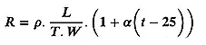
p = resistivity of copper | a = temperature coefficient of copper | T = trace thickness
W = trace width | L = trace length | t = temperature
In addition to trace width, the shape of the trace also affects signal reflection.
Asymmetrical trace dimensions and sharp bends can cause signal reflection, leading to signal distortion.
In multilayer PCBs, power signal traces are typically placed on the top layer to improve heat dissipation.
On the other hand, data signal traces are placed on internal layers to prevent EMI and environmental noise.
Practical Example—Optimizing Trace Width for a DC Motor Power Path
The following example illustrates the process of calculating a specific trace width for a power signal that transmits current from a power supply component to a peripheral device.
The primary objective is to calculate the minimum trace width for the power path of a DC motor.
The power path begins at the fuse, passes through the H-bridge (a component used to manage power delivery to the DC motor windings), and ends at the motor’s connector.
The average continuous maximum current required by the DC motor is approximately 2 amps.
PCB traces act as resistors; the longer and narrower the trace, the greater the resistance.
If the trace is not properly defined, high current may damage the trace and/or cause a significant voltage drop across the motor (resulting in reduced speed).
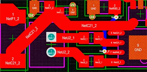
The NetC21_2 shown in Figure 3 is approximately 0.8 inches long and must carry a maximum current of 2 A.
If we assume some general conditions—such as 1-ounce copper cladding during normal operation and ambient room temperature—we need to calculate the minimum trace width and the expected voltage drop at that width.
Role of PCB Trace Width in Layout
PCB trace width affects the electrical performance of printed circuit boards, including:
- Signal integrity
- Power integrity
Signal Integrity
Using different trace widths can significantly improve signal integrity and control signal interference, crosstalk, electromagnetic interference, and other issues.
Controlled Impedance Routing
When dealing with certain high-speed signals, they must be routed at specific widths to ensure impedance control.
Trace widths must be correctly calculated based on the following factors:
- Board’s dielectric material.
- Spacing from other signals.
- Copper weight.
Microstrip and Stripline
For sensitive high-speed transmission lines, coupling to a reference ground plane is required to shield the traces.
A stripline configuration refers to an internal routing layer sandwiched between two ground planes.
On the other hand, a microstrip configuration refers to traces on the exterior of the PCB and the adjacent plane beneath them.
Analog Routing
Analog signals should be routed short and direct, with additional width to maintain low trace impedance.
For analog circuits, it is best to minimize the use of vias.
Power Integrity
1) Short and Direct Routing
It is important to keep traces short to avoid additional noise. Rounded corners, as opposed to right angles, are also preferred.
2) Use Wide Traces
To reduce inductance and crosstalk, it is advisable to use wide traces for power routing.
3) Current and Thermal Considerations
Power traces carry different current levels depending on the network being routed.
Additionally, it is important to consider the heat generated by the traces as current flows through them.
Outer-layer power traces can also benefit from air cooling.
Case 1—Routing High-Speed USB Lines
For digital designs with high-speed communication, specific spacing and tuned lengths may be required to minimize crosstalk, coupling, and reflections.
Some common applications include USB-based serial differential signals and RAM-based parallel differential signals.
Typically, USB 2.0 requires differential pairs routed for speeds of 480 Mbit/s (USB High-Speed mode) or higher.
This is partly because high-speed USB typically operates at much lower voltages and differential levels, bringing the overall signal level closer to the background noise.
Three important factors must be considered when routing high-speed USB traces: trace width, trace spacing, and trace length.
All of these are important, but the most critical of the three is ensuring that the lengths of the two traces match as closely as possible. As a general rule of thumb,
if the length difference between traces exceeds 50 mils (for high-speed USB), the risk of reflections—which can lead to poor communication—increases significantly.
A 902-ohm matched impedance is a common specification for differential pair routing; to achieve this, trace width and spacing should be optimized.
The figure below shows an example of a differential pair routed for a high-speed USB interface, featuring 12-mil-wide traces with 15-mil spacing.

Interfaces for memory-based components that include parallel interfaces—such as DDR3-SDRAM—are subject to stricter constraints regarding trace length.
Most high-end PCB design software includes length-adjustment features that optimize trace lengths to match all relevant signals in a parallel bus.
The figure below shows an example of a DDR3 layout with length-adjusted traces.

Case 2—In-Ground Traces and Planes
Some applications with noise-sensitive components (such as wireless chips or antennas) may require additional protection.
Designing traces and planes with embedded ground vias can greatly help minimize coupling picked up from nearby traces or planes, as well as off-board signals infiltrating the board edges.
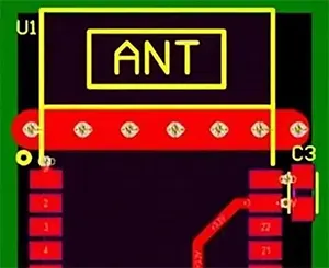
The figure below shows an example of a Bluetooth module placed near the edge of the board, with its antenna (marked with the silkscreen label “ANT”) located outside a thick trace containing embedded vias connected to the ground plane.
This helps isolate the antenna from other on-board circuits and planes.
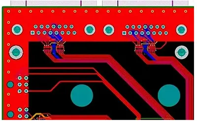
Another method involving ground via-embedded planes (or, in this example, a polygonal ground plane) can be used to protect the circuit on the board from external, off-board radio frequency signals.
The figure below shows a noise-sensitive PCB with a ground via-embedded plane around the perimeter of the board.
Various Trace Widths and Thicknesses
It is common for PCBs to include traces of various widths, as these depend on the signal requirements (as shown in the figure below).
The thinner traces shown are used for general-purpose TTL (Transistor-Transistor Logic) level signals, which have no special requirements for high current or noise protection.
These will be the most common types of traces on a circuit board.

The wider traces have been optimized for current-carrying capacity and are used for peripherals or power-related functions that require higher power, such as fans, motors, and general power delivery to lower-level components.
The upper-left corner of the figure even shows a differential signal (USB High-Speed), where specific spacing and widths are defined to meet the impedance requirements of the 902 standard.
The figure below shows a slightly denser 6-layer PCB and a BGA (ball grid array) component that requires finer traces.

Line Width Specifications in PCB Manufacturing
As a general rule, the following trace-related specifications begin to drive up the manufacturing costs of bare PCBs.
Due to stricter PCB tolerances and the high-end equipment required to manufacture, inspect, or test PCBs, costs can become quite high:
Trace widths less than 5 mils (0.005″)
Trace spacing less than 5 mils
Through-holes with a diameter less than 8 mils
Trace thickness thinner than or thicker than 1 ounce (equivalent to 1.4 mils)
Differential pairs and controlled trace length or impedance
High-density designs that occupy a significant PCB footprint (such as ultra-fine-pitch BGAs or parallel buses with a high number of signals) may require trace widths as thin as 2.5 mils and special types of through-holes, such as laser-drilled microvia with a diameter of 6 mils or smaller.
In contrast, some high-power designs may require very large traces or planes that span an entire layer and use a pour thickness greater than the standard.
Space-constrained applications may require very thin boards comprising several layers and a limited copper pour thickness of half an ounce (0.7 mils).
In other cases, high-speed communication designs between peripheral devices may require traces with controlled impedance, as well as specific widths and spacing between them, to minimize reflections and inductive coupling.
Alternatively, a design may require specific lengths to match other relevant signals on the bus.
High-voltage applications require certain safety features, such as minimizing the distance between two exposed differential signals to prevent arcing.

