With the rapid development of technologies such as 5G, radar, and satellite communications, there is a growing demand for high-frequency, high-density interconnect (HDI) boards that require extremely high levels of signal integrity.
These products strive for the utmost in surface flatness, signal transmission performance, reliability, and routing density;
Consequently, the plating-over-filled-via (POFV) process is widely adopted.
This process involves filling through-holes with resin after plating and then plating the surface again to create a flat surface suitable for routing.
POFV has become a core manufacturing process for modern high-end printed circuit boards (PCBs), particularly high-frequency, high-density interconnect boards, and can significantly enhance a product’s signal transmission performance, reliability, and routing density.
However, electroplating on a non-metallic resin surface carries the risk of plating delamination, a risk that becomes particularly pronounced after high-temperature reflow soldering.
To prevent delamination in POFV, this paper analyzes PCBs incorporating the POFV process from the perspectives of defect phenomena, failure mechanisms, process parameters, and engineering design.
Researchers validate the analysis through comparative testing and propose corresponding improvement strategies.
Failure Analysis
Researchers summarize the failure mechanism of delamination between the POFV plating layer and via-filling resin on PCBs as follows.
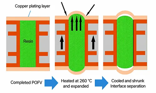
During thermal expansion at high temperatures, the thick via copper and the thick inner layer copper form a relatively rigid structure that restricts the via-filling resin from releasing stress in all directions.
This causes the expansion stress to accumulate primarily along the Z-axis, resulting in significant internal stress in that direction and triggering deformation.
Researchers relate the magnitude of this deformation to the thickness of the POFV copper layer.
Due to the significant deformation, the tensile stress generated during the cooling and contraction phase exceeds the interfacial bonding strength, leading to delamination.
The probability of such delamination occurring is significantly higher than in boards with conventional via copper thicknesses.
This is particularly true for high-frequency materials, which have a lower coefficient of thermal expansion (CTE) and thicker via copper, placing higher demands on thermal expansion compatibility and POFV bonding strength.
Thick-hole-copper structures are more prone to POFV delamination.
Furthermore, the thinner the POFV cap copper, the weaker its ability to resist expansion deformation; the greater the stress generated during contraction, and the higher the risk of delamination.
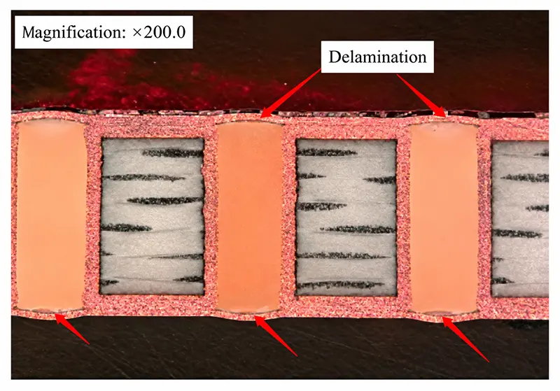
Figure 1 illustrates this failure mode, and Figure 2 shows the actual failure conditions.
Improvement Plan and Validation Analysis
Improvement Plan Design
1. Design of Comparative Factor Analysis
Researchers analyzed POFV failure mechanisms above. They plan validation experiments.
The goal is to boost reliability for PCBs made with the high-frequency POFV process.
These experiments target two key factors. The first is CTE compatibility between high-frequency substrates and via-filling resin. The second is the pretreatment process for via-filling resin.
Optimization of POFV copper plating thickness and optimization of via-filling resin performance.
Researchers conduct these experiments to identify the optimal combination of process steps and resin materials, and to validate it under reflow soldering conditions to achieve the best solution.
The specific plan is shown in Table 1.
| Test Plan | Comparison Factor | Validation Test Method | Number of Test Specimens |
|---|---|---|---|
| Plan 1 | Two types of potting resin, Resin A and Resin B, with different coefficients of thermal expansion (CTEs) | Compare the effects of two potting resins with different CTEs on via plugging. | 16 specimens, with 8 specimens for each condition. |
| Plan 2 | Two different via-plugging pretreatment parameters, Parameter 1 and Parameter 2 | Compare two different via-plugging pretreatment methods. | Evenly divide the specimens from Plan 1 between the two conditions, with 8 specimens per condition. |
| Plan 3 | Two different POFV pretreatment methods, Method 1 and Method 2 | Compare two sets of parameters for the baking plate used before immersion tinning. | Evenly divide the specimens from Plan 2 between the two conditions, with 8 specimens per condition. |
| Plan 4 | Two different POFV coating thicknesses, Thickness 1 and Thickness 2 | Compare two different coating thicknesses. | Evenly divide the specimens from Plan 3 between the two conditions, with 8 specimens per condition. |
Table 1. Validation Test Plan
2. Design Validation Using Different Contrast Factor Matrices
This experiment employed a systematic multivariate design, with four factors each having two variables.
By combining all factors (2×2×2×2), researchers established 16 unique process conditions and assigned one test plate to each condition (see Table 2).
Manufacturers fabricated all test boards from 0.54 mm-thick hydrocarbon high-frequency material; each board contained 24 cells and plug holes with a diameter of 0.25 mm.
The design allowed researchers to validate each combination independently.
This design enables comprehensive coverage and efficient validation of key variables such as resin properties, pretreatment processes, thermal curing treatments, and plating thickness.
| Parameter | Resin A | Resin B |
|---|---|---|
| Resin Type | Resin A | Resin B |
| Quantity (Panels) | 8 | 8 |
1. Hole Plugging Pretreatment
| Parameter | Resin A | Resin B |
|---|---|---|
| Parameter 1 | 4 Panels | 4 Panels |
| Parameter 2 | 4 Panels | 4 Panels |
2. Copper Deposition Pretreatment
| Hole Plugging Parameter | Copper Deposition Method | Resin A (Panels) | Resin B (Panels) |
|---|---|---|---|
| Parameter 1 | Method 1 | 2 | 2 |
| Parameter 1 | Method 2 | 2 | 2 |
| Parameter 2 | Method 1 | 2 | 2 |
| Parameter 2 | Method 2 | 2 | 2 |
3. POFV Copper Thickness
| Hole Plugging Parameter | Copper Deposition Method | POFV Copper Thickness | Resin A (Panels) | Resin B (Panels) |
|---|---|---|---|---|
| Parameter 1 | Method 1 | Thickness 1 | 1 | 1 |
| Parameter 1 | Method 1 | Thickness 2 | 1 | 1 |
| Parameter 1 | Method 2 | Thickness 1 | 1 | 1 |
| Parameter 1 | Method 2 | Thickness 2 | 1 | 1 |
| Parameter 2 | Method 1 | Thickness 1 | 1 | 1 |
| Parameter 2 | Method 1 | Thickness 2 | 1 | 1 |
| Parameter 2 | Method 2 | Thickness 1 | 1 | 1 |
| Parameter 2 | Method 2 | Thickness 2 | 1 | 1 |
| Total | 8 | 8 |
Table 2. Test Panel Validation Matrix
3. Explanation of Different Comparison Factors
(1) Filler-reinforced Resin Materials.
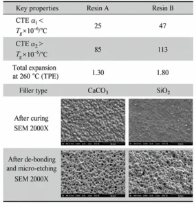
The fundamental difference between Type A and Type B resins lies in their thermodynamic compatibility and filler systems.
Type A uses resins with a lower CTE, while Type B uses resins with a higher CTE.
The CTE values of the resins and the filler specifications are shown in Table 3.
(2) Pre-treatment Process for Plugging Holes.
Parameter 1 is a super-roughening treatment, which roughens the copper plating layer inside the holes;
Parameter 2 is a board grinding treatment, which does not affect the copper layer inside the holes.
(3) Pre-treatment Process for Copper Plating.
Method 1 involves a vertical oven at 120 °C for 60 minutes; Method 2 involves no oven drying.
(4) POFV Copper Plating.
Thickness 1 corresponds to a copper layer of 10–18 μm; Thickness 2 corresponds to a copper layer of 19–28 μm.
Operators select copper plating parameters that form a dense cap layer in the key POFV process steps.
Final reliability verification simulates the extreme thermal shock conditions of actual reflow soldering;
Engineers design this full set of parameters to operate synergistically.
They verify the specific effects of each process variable on suppressing thermomechanical stress and improving interfacial adhesion, and thereby systematically identify the optimal process combination.
Experimental Procedure
Material Cutting → Drilling → Copper Plating → Electroplating → Super-roughening/Board Grinding (Verification Option) → Board Baking Before Via Filling (Validation Option) → Resin Via Filling → Automated Optical Inspection (AOI) of Resin → Removal of Resin Residue → Secondary Copper Plating → Full-Board Plating → Outer Layer Traces → Etching → Solder Mask Application → 5 Reflow Soldering Cycles → Slice Inspection.
Validation Results
Based on the aforementioned process scheme, validation procedure, and validation parameters, researchers conducted a systematic comparison focusing on four key process variables.
They used 8 test boards for each set of conditions and validated 24 slices. Figure 4 presents the final test board results.
The validation results indicate that the integrated process scheme is highly effective in preventing POFV delamination, including: selecting a resin with low CTE and CaCO₃ filler;
Performing ultra-coarse finishing on the copper surface prior to plugging;
Thoroughly baking the board to remove moisture before copper plating on the POFV; and appropriately increasing the POFV plating thickness.
From a materials science perspective, the effectiveness of the above scheme stems from the fundamental differences between Type A resin (low CTE) and Type B resin (high CTE).
Type A resin has a lower CTE and offers better thermal compatibility with high-frequency substrates, fundamentally reducing interfacial thermal stress;
It is therefore the preferred choice for high-reliability POFV applications.
The CaCO₃ filler in Type A resin also aids in processing, and the rougher surface resulting from micro-etching after resin removal enhances adhesion to the plating layer.
In contrast, the higher CTE of Type B resin increases the risk of thermal mismatch with the substrate.
Although SiO₂ filler can improve rigidity, it is more suitable for applications that are less sensitive to thermal stress.
Therefore, to ensure the long-term reliability of high-frequency products, selecting Type A resin with a low CTE is the optimal solution for controlling the risk of delamination.
| Plan | Comparison Factors | Test Results | Conclusions |
|---|---|---|---|
| Plan 1 | Resins with Different CTE Values and Fillers | SiO₂ filler, high-CTE resin: 8 delamination cases; defect rate: 30.0%. CaCO₃ filler, low-CTE resin: No delamination; defect rate: 0%. | CaCO₃ filler and low-CTE properties can reduce the risk of POFV delamination and improve bonding strength. |
| Plan 2 | Different Hole Plugging Pretreatment Methods | Without micro-roughening treatment: 12 delamination cases; defect rate: 50.0%. With micro-roughening treatment: 4 delamination cases; defect rate: 16.7%. | Micro-roughening pretreatment before hole plugging can enhance adhesion between resin and copper, reducing the risk of delamination. |
| Plan 3 | Different POFV Pretreatment Methods | Without baking: 8 delamination cases; defect rate: 33.3%. With baking before copper deposition: 3 delamination cases; defect rate: 16.7%. | Baking before POFV copper deposition can remove moisture from the holes and reduce the risk of delamination. |
| Plan 4 | Different POFV Plating Thicknesses | Plating thickness 10–15 μm: 14 delamination cases; defect rate: 58.3%. Plating thickness ≥16 μm: 2 delamination cases; defect rate: 8.3%. | Thicker POFV copper plating (≥16 μm) provides greater resistance to high-temperature thermal shock and reduces the risk of delamination. |
Table 5. Validation Plans and Results
Conclusion
Through analysis and validation, researchers conclude that systematic optimization of process parameters can effectively prevent POFV delamination in PCBs.
Specifically, this includes: selecting a resin with low CTE (CaCO₃ filler) for via filling to improve thermal matching with the substrate;
Performing an ultra-roughening treatment on the copper layer lining the via walls prior to resin filling to enhance interfacial adhesion;
Baking at 120 °C for 60 minutes prior to POFV copper plating to thoroughly remove moisture from the holes;
And controlling the POFV copper plating thickness to 19–28 μm or thicker to enhance the plating’s resistance to high-temperature shock.
The validation results indicate that this comprehensive approach significantly reduces the risk of delamination and provides effective assurance for the reliability of POFV in high-frequency PCBs.